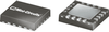
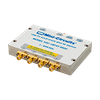
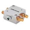
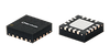
The VSWA2-63DR+ is a high isolation absorptive SPDT switch with integral CMOS driver, operates with single positive supply voltage while consuming, 12 µA typical. It has been designed for very wideband operation of 500 to 6000 MHz for 50Ω systems and yet is usable in 75Ω systems with degraded return loss. This switch is usable over an extended frequencies from 300 kHz to 500 MHz with reflective switch performance. It is packaged in a tiny 4 x 4 x 0.9 mm package and is rated MSL1 and class 1A ESD. SIMPLIFIED SCHEMATIC AND PAD DESCRIPTION V RF1 DD Control GND RF COM GND GND RF2 Pad Function Description Number RF COM 3 RF Common/SUM Port, Requires DC block (see Fig. 2) RF1 12 RF Out #1/In Port #1, Requires DC block (see Fig. 2) RF2 9 RF Out #2/In Port #2, Requires DC block (see Fig. 2) Control 2 CMOS Control IN V 1 Supply Voltage DD 4,5,6,7,8,10,11 GND RF Ground 13,14,15,16 & Paddle REV. G ECO-026600 VSWA2-63DR+ MCL NY 260429 www.minicircuits.com P.O. Box 350166, Brooklyn, NY 11235-0003 (718) 934-4500 sales@minicircuits.c
om PAGE 1 OF 5 DNG DNG DNG DNG DNG DNG DNG DNG 1 12 2 11 3 10 4 9 61 5 51 6 41 7 31 8 RF Common Cblock DUT RF Section Cblock Cblock RF1 RF2 Paddle Internal CMOS Driver Control V DD SURFACE MOUNT SPDT RF Switch VSWA2-63DR+ 50Ω 500 to 6000 MHz Absorptive RF Switch with Internal Driver Single Supply Voltage, +3 V to +5 V RF ELECTRICAL SPECIFICATIONS1, T = +25°C, V = +3 V TO +5 V AMB DD Parameter Condition (MHz) Min. Typ. Max. Units Frequency Range 500 6000 MHz 0.3-500 – 0.7 – 500-2000 – 0.7 1.3 Insertion Loss2 2000-3000 – 0.8 1.5 dB 3000-4000 – 0.9 1.5 4000-6000 – 1.0 1.9 0.3-500 – 73 – 500-2000 56 66 – Isolation Between Common Port and RF1/RF2 Ports 2000-3000 50 64 – dB 3000-4000 45 58 – 4000-6000 38 54 – 0.3-500 – 74 – 500-1000 50 60 – 1000-2000 45 56 – Isolation Between RF1 and RF2 Ports dB 2000-3000 40 52 – 3000-4000 38 50 – 4000-6000 34 46 – 0.3-500 – 24 – 500-2000 – 23 – Return Loss 2000-3000 – 23 – dB (ON STATE) 3000-4000 – 22 – 4000-6000 – 20 – 500-2000 – 23 – Return Loss @ RF1/RF2 Ports 2000-3000 – 33 – dB (OFF STATE) 3000-4000 – 23 – 4000-6000 – 24 – 500-2000 – +46 – V = +3 V DD 2000-6000 – +40 – Input IP3 dBm 500-2000 – +50 – V = +5 V DD 2000-6000 – +44 – 500-2000 – +24 – 1 dB, V = +3 V DD 2000-6000 – +22 – Input Compression3 dBm 500-2000 – +30 – 0.2 dB, V = +5 V DD 2000-6000 – +27 – 1. Tested on Mini-Circuit’s test board TB-486+, using Agilent’s N5230A network analyzer (see Characterization Test Circuit, Fig. 1). 2. Insertion loss values are de-embedded from test board loss. 3. Do not exceed RF input power as shown in Absolute Maximum Rating table. DC ELECTRICAL SPECIFICATIONS Parameter Min. Typ. Max. Units V , Supply Voltage +3 – +5 V DD Supply Current (V = +5 V)4 – 50 – µA DD Control Voltage Low 0 – +0.5 V Control Voltage High5 +2.76 – V V DD Control Current – 5 – µA 4. Supply current increases with switching repetition rate. See graph. 5. CMOS interface. Latch up condition may occur when logic high signal is applied prior to power supply. 6. +3.5 V for V = +4 V to +5 V DD www.minicircuits.com P.O. Box 350166, Brooklyn, NY 11235-0003 (718) 934-4500 sales@minicircuits.c
om PAGE 2 OF 5 SURFACE MOUNT SPDT RF Switch VSWA2-63DR+ 50Ω 500 to 6000 MHz Absorptive RF Switch with Internal Driver Single Supply Voltage, +3 V to +5 V SWITCHING SPECIFICATIONS Parameter Min. Typ. Max. Units Rise/Fall Time (10 to 90% or 90 to 10% RF) – 23 – ns Switching Time, 50% CTRL to 90/10% RF – 35 – ns Video Feed-Through, (Control 0 to +3 V, Freq. = 500 KHz, V = +5 V) – 25 – mV DD P.P
The VSWA2-63DR+ is a high isolation absorptive SPDT switch with integral CMOS driver, operates with single positive supply voltage while consuming, 12 µA typical. It has been designed for very wideband operation of 500 to 6000 MHz for 50Ω systems and yet is usable in 75Ω systems with degraded return loss. This switch is usable over an extended frequencies from 300 kHz to 500 MHz with reflective switch performance. It is packaged in a tiny 4 x 4 x 0.9 mm package and is rated MSL1 and class 1A ESD. SIMPLIFIED SCHEMATIC AND PAD DESCRIPTION V RF1 DD Control GND RF COM GND GND RF2 Pad Function Description Number RF COM 3 RF Common/SUM Port, Requires DC block (see Fig. 2) RF1 12 RF Out #1/In Port #1, Requires DC block (see Fig. 2) RF2 9 RF Out #2/In Port #2, Requires DC block (see Fig. 2) Control 2 CMOS Control IN V 1 Supply Voltage DD 4,5,6,7,8,10,11 GND RF Ground 13,14,15,16 & Paddle REV. G ECO-026600 VSWA2-63DR+ MCL NY 260429 www.minicircuits.com P.O. Box 350166, Brooklyn, NY 11235-0003 (718) 934-4500 sales@minicircuits.com PAGE 1 OF 5 DNG DNG DNG DNG DNG DNG DNG DNG 1 12 2 11 3 10 4 9 61 5 51 6 41 7 31 8 RF Common Cblock DUT RF Section Cblock Cblock RF1 RF2 Paddle Internal CMOS Driver Control V DD SURFACE MOUNT SPDT RF Switch VSWA2-63DR+ 50Ω 500 to 6000 MHz Absorptive RF Switch with Internal Driver Single Supply Voltage, +3 V to +5 V RF ELECTRICAL SPECIFICATIONS1, T = +25°C, V = +3 V TO +5 V AMB DD Parameter Condition (MHz) Min. Typ. Max. Units Frequency Range 500 6000 MHz 0.3-500 – 0.7 – 500-2000 – 0.7 1.3 Insertion Loss2 2000-3000 – 0.8 1.5 dB 3000-4000 – 0.9 1.5 4000-6000 – 1.0 1.9 0.3-500 – 73 – 500-2000 56 66 – Isolation Between Common Port and RF1/RF2 Ports 2000-3000 50 64 – dB 3000-4000 45 58 – 4000-6000 38 54 – 0.3-500 – 74 – 500-1000 50 60 – 1000-2000 45 56 – Isolation Between RF1 and RF2 Ports dB 2000-3000 40 52 – 3000-4000 38 50 – 4000-6000 34 46 – 0.3-500 – 24 – 500-2000 – 23 – Return Loss 2000-3000 – 23 – dB (ON STATE) 3000-4000 – 22 – 4000-6000 – 20 – 500-2000 – 23 – Return Loss @ RF1/RF2 Ports 2000-3000 – 33 – dB (OFF STATE) 3000-4000 – 23 – 4000-6000 – 24 – 500-2000 – +46 – V = +3 V DD 2000-6000 – +40 – Input IP3 dBm 500-2000 – +50 – V = +5 V DD 2000-6000 – +44 – 500-2000 – +24 – 1 dB, V = +3 V DD 2000-6000 – +22 – Input Compression3 dBm 500-2000 – +30 – 0.2 dB, V = +5 V DD 2000-6000 – +27 – 1. Tested on Mini-Circuit’s test board TB-486+, using Agilent’s N5230A network analyzer (see Characterization Test Circuit, Fig. 1). 2. Insertion loss values are de-embedded from test board loss. 3. Do not exceed RF input power as shown in Absolute Maximum Rating table. DC ELECTRICAL SPECIFICATIONS Parameter Min. Typ. Max. Units V , Supply Voltage +3 – +5 V DD Supply Current (V = +5 V)4 – 50 – µA DD Control Voltage Low 0 – +0.5 V Control Voltage High5 +2.76 – V V DD Control Current – 5 – µA 4. Supply current increases with switching repetition rate. See graph. 5. CMOS interface. Latch up condition may occur when logic high signal is applied prior to power supply. 6. +3.5 V for V = +4 V to +5 V DD www.minicircuits.com P.O. Box 350166, Brooklyn, NY 11235-0003 (718) 934-4500 sales@minicircuits.com PAGE 2 OF 5 SURFACE MOUNT SPDT RF Switch VSWA2-63DR+ 50Ω 500 to 6000 MHz Absorptive RF Switch with Internal Driver Single Supply Voltage, +3 V to +5 V SWITCHING SPECIFICATIONS Parameter Min. Typ. Max. Units Rise/Fall Time (10 to 90% or 90 to 10% RF) – 23 – ns Switching Time, 50% CTRL to 90/10% RF – 35 – ns Video Feed-Through, (Control 0 to +3 V, Freq. = 500 KHz, V = +5 V) – 25 – mV DD P.P