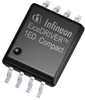
650 V, 2.5 A high current high-side and low-side gate driver IC with integrated bootstrap diode in DSO-8 package
650 V high and low side gate driver with high current, and high speed to drive MOSFETand IGBT, with typical 2.5 A sink and source current in DSO-8 package. The DSO-14 package version for bigger creepage is also available: 2ED21814S06J.
Based on Infineon’s SOI-technology, having excellent ruggedness and noise immunity against negative transient voltages on VS pin. No parasitic thyristor structures present in the device, hence no parasitic latch up at all temperature and voltage conditions.
Summary of Features
Operating voltages (VS node) upto + 650 V
Negative VS transient immunity of 100 V
Integrated ultra-fast, low resistance bootstrap diode, lower the BOM cost
Floating channel designed for bootstrap operation
Maximum supply voltage of 25 V
Independent under voltage lockout (UVLO) for both channels
200 ns propagation delay
HIN, LIN input logic
Logic Operational up to –11 V on VS Pin
Negative Voltage Tolerance On Inputs of –5 V
The floating channel can be used to drive an N-channel MOSFET, SiC MOSFET or IGBT in the high side configuration
Benefits
High current gate driver - suitable for high current power device, and high frequency application
Integrated bootstrap diode (BSD) - Space saving, reduced BOM cost, smaller PCB at lower cost with simpler design
50% lower level-shift losses
Excellent ruggedness and noise immunity against negative transient voltages (-100 V) on VS pin
Applications
Commercial HVAC
Cordless power tools and outdoor power equipment
Home appliances
Motor Control
Power conversion
Find our Variations for 2ED2181S06F
Part No Package Input logic Interlock Deadtime 2ED21814S06J DSO - 14 HIN, LIN No
None
2ED2182S06F
DSO - 8 HIN, LIN Yes Internal 400 ns
2ED21824S06J
DSO - 14 HIN, LIN
Yes
Programmable 400 ns - 5000 ns
2ED2183S06F DSO - 8 HIN, /LIN
Yes
Internal 400 ns
2ED21834S06J DSO – 14 HIN, /LIN
Yes
Programmable 400 ns - 5000 ns
2ED2184S06F DSO - 8 IN, /SD
Yes
Internal 400 ns
2ED21844S06J DSO – 14
IN, /SD
Yes
Programmable 400 ns - 5000 ns
Part No Package Input logic Interlock Deadtime
Designers who used this product also designed with
S26KS512SDPBHN020 | HYPERFLASH™
BSC110N15NS5 | N-Channel Power MOSFET
IMBF170R650M1 | Silicon Carbide MOSFET Discretes
1EDN7126U | Gate driver ICs
S25FL128LAGMFI010 | Quad SPI Flash
IR3899AMTRPBF | Integrated POL Voltage Regulators
BSC098N10NS5 | N-Channel Power MOSFET
BSC074N15NS5 | N-Channel Power MOSFET
BSC040N10NS5 | N-Channel Power MOSFET
TLF35584QVVS2 | OPTIREG™ PMIC
BSZ440N10NS3 G | N-Channel Power MOSFET
BSZ123N08NS3 G | N-Channel Power MOSFET
S26KS512SDPBHN020 | HYPERFLASH™
BSC110N15NS5 | N-Channel Power MOSFET
IMBF170R650M1 | Silicon Carbide MOSFET Discretes
1EDN7126U | Gate driver ICs
S25FL128LAGMFI010 | Quad SPI Flash
IR3899AMTRPBF | Integrated POL Voltage Regulators
BSC098N10NS5 | N-Channel Power MOSFET
BSC074N15NS5 | N-Channel Power MOSFET
1 2 3
650 V, 2.5 A high current high-side and low-side gate driver IC with integrated bootstrap diode in DSO-8 package
650 V high and low side gate driver with high current, and high speed to drive MOSFETand IGBT, with typical 2.5 A sink and source current in DSO-8 package. The DSO-14 package version for bigger creepage is also available: 2ED21814S06J.
Based on Infineon’s SOI-technology, having excellent ruggedness and noise immunity against negative transient voltages on VS pin. No parasitic thyristor structures present in the device, hence no parasitic latch up at all temperature and voltage conditions.
Summary of Features
- Operating voltages (VS node) upto + 650 V
- Negative VS transient immunity of 100 V
- Integrated ultra-fast, low resistance bootstrap diode, lower the BOM cost
- Floating channel designed for bootstrap operation
- Maximum supply voltage of 25 V
- Independent under voltage lockout (UVLO) for both channels
- 200 ns propagation delay
- HIN, LIN input logic
- Logic Operational up to –11 V on VS Pin
- Negative Voltage Tolerance On Inputs of –5 V
- The floating channel can be used to drive an N-channel MOSFET, SiC MOSFET or IGBT in the high side configuration
Benefits
- High current gate driver - suitable for high current power device, and high frequency application
- Integrated bootstrap diode (BSD) - Space saving, reduced BOM cost, smaller PCB at lower cost with simpler design
- 50% lower level-shift losses
- Excellent ruggedness and noise immunity against negative transient voltages (-100 V) on VS pin
Applications
- Commercial HVAC
- Cordless power tools and outdoor power equipment
- Home appliances
- Motor Control
- Power conversion
Find our Variations for 2ED2181S06F
Part No Package Input logic Interlock Deadtime
2ED21814S06J DSO - 14 HIN, LIN No
None
2ED2182S06F
DSO - 8 HIN, LIN Yes Internal 400 ns
2ED21824S06J
DSO - 14 HIN, LIN
Yes
Programmable 400 ns - 5000 ns
2ED2183S06F DSO - 8 HIN, /LIN
Yes
Internal 400 ns
2ED21834S06J DSO – 14 HIN, /LIN
Yes
Programmable 400 ns - 5000 ns
2ED2184S06F DSO - 8 IN, /SD
Yes
Internal 400 ns
2ED21844S06J DSO – 14
IN, /SD
Yes
Programmable 400 ns - 5000 ns
Part No Package Input logic Interlock Deadtime
Designers who used this product also designed with
- S26KS512SDPBHN020 |
HYPERFLASH™
- BSC110N15NS5 |
N-Channel Power MOSFET
- IMBF170R650M1 |
Silicon Carbide MOSFET Discretes
- 1EDN7126U |
Gate driver ICs
- S25FL128LAGMFI010 |
Quad SPI Flash
- IR3899AMTRPBF |
Integrated POL Voltage Regulators
- BSC098N10NS5 |
N-Channel Power MOSFET
- BSC074N15NS5 |
N-Channel Power MOSFET
- BSC040N10NS5 |
N-Channel Power MOSFET
- TLF35584QVVS2 |
OPTIREG™ PMIC
- BSZ440N10NS3 G |
N-Channel Power MOSFET
- BSZ123N08NS3 G |
N-Channel Power MOSFET
- S26KS512SDPBHN020 |
HYPERFLASH™
- BSC110N15NS5 |
N-Channel Power MOSFET
- IMBF170R650M1 |
Silicon Carbide MOSFET Discretes
- 1EDN7126U |
Gate driver ICs
- S25FL128LAGMFI010 |
Quad SPI Flash
- IR3899AMTRPBF |
Integrated POL Voltage Regulators
- BSC098N10NS5 |
N-Channel Power MOSFET
- BSC074N15NS5 |
N-Channel Power MOSFET
1
2
3