The 74LV4053-Q100 is a triple single-pole double-throw (SPDT) analog switch, suitable for use as an analog or digital multiplexer/demultip
lexer. It is a low-voltage Si-gate CMOS device and is pin and function compatible with the 74HC4053-Q100 and 74HCT4053-Q100. Each switch has a digital select input (Sn), two independent inputs/outputs (nY0 and nY1) and a common input/output (nZ). All three switches share an enable input (E). A HIGH on Ecauses all switches into the high-impedance OFF-state, independent of Sn.
VCC and GND are the supply voltage connections for the digital control inputs (Sn and E). The VCC to GND range is 1 V to 6 V. The analog inputs/outputs (nY0, nY1 and nZ) can swing between VCC as a positive limit and VEE as a negative limit. VCC - VEE may not exceed 6 V. For operation as a digital multiplexer/demultip
lexer, VEE is connected to GND (typically ground). VEE and VSS are the supply voltage connections for the switches.
This product has been qualified to the Automotive Electronics Council (AEC) standard Q100 (Grade 1) and is suitable for use in automotive applications.
Features and benefits
Automotive product qualification in accordance with AEC-Q100 (Grade 1)
Specified from -40 °C to +85 °C and from -40 °C to +125 °C
Optimized for low-voltage applications: 1.0 V to 3.6 V
Accepts TTL input levels between VCC = 2.7 V and VCC = 3.6 V
Low ON resistance:
180 Ω (typical) at VCC - VEE = 2.0 V
100 Ω (typical) at VCC - VEE = 3.0 V
75 Ω (typical) at VCC - VEE = 4.5 V
Logic level translation:
To enable 3 V logic to communicate with ±3 V analog signals
Typical ‘break before make’ built in
ESD protection:
HBM: ANSI/ESDA/JEDEC JS-001 class 2 exceeds 2000 V
CDM: ANSI/ESDA/JEDEC JS-002 class C3 exceeds 1000 V
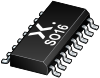
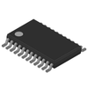
Multiple package options
DHVQFN package with Side-Wettable Flanks enabling Automatic Optical Inspection (AOI) of solder joints
The 74LV4053-Q100 is a triple single-pole double-throw (SPDT) analog switch, suitable for use as an analog or digital multiplexer/demultiplexer. It is a low-voltage Si-gate CMOS device and is pin and function compatible with the 74HC4053-Q100 and 74HCT4053-Q100. Each switch has a digital select input (Sn), two independent inputs/outputs (nY0 and nY1) and a common input/output (nZ). All three switches share an enable input (E). A HIGH on Ecauses all switches into the high-impedance OFF-state, independent of Sn.
VCC and GND are the supply voltage connections for the digital control inputs (Sn and E). The VCC to GND range is 1 V to 6 V. The analog inputs/outputs (nY0, nY1 and nZ) can swing between VCC as a positive limit and VEE as a negative limit. VCC - VEE may not exceed 6 V. For operation as a digital multiplexer/demultiplexer, VEE is connected to GND (typically ground). VEE and VSS are the supply voltage connections for the switches.
This product has been qualified to the Automotive Electronics Council (AEC) standard Q100 (Grade 1) and is suitable for use in automotive applications.
Features and benefits
- Automotive product qualification in accordance with AEC-Q100 (Grade 1)
- Specified from -40 °C to +85 °C and from -40 °C to +125 °C
- Optimized for low-voltage applications: 1.0 V to 3.6 V
- Accepts TTL input levels between VCC = 2.7 V and VCC = 3.6 V
- Low ON resistance:
- 180 Ω (typical) at VCC - VEE = 2.0 V
- 100 Ω (typical) at VCC - VEE = 3.0 V
- 75 Ω (typical) at VCC - VEE = 4.5 V
- Logic level translation:
- To enable 3 V logic to communicate with ±3 V analog signals
- Typical ‘break before make’ built in
- ESD protection:
- HBM: ANSI/ESDA/JEDEC JS-001 class 2 exceeds 2000 V
- CDM: ANSI/ESDA/JEDEC JS-002 class C3 exceeds 1000 V
- Multiple package options
- DHVQFN package with Side-Wettable Flanks enabling Automatic Optical Inspection (AOI) of solder joints