Integrated Device Technology PCI Express Jitter Attenuator 9DB306BFLFT

Description
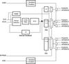
The 9DB306 is a high performance 1-to-6 Differential-to- LVPECL Jitter Attenuator designed for use in PCI Express®™ systems. In some PCI Express® systems, such as those found in desktop PCs, the PCI Express® clocks are generated from a low bandwidth, high phase noise PLL frequency synthesizer. In these systems, a zero delay buffer may be required to attenuate high frequency random and deterministic jitter components from the PLL synthesizer and from the system board. The 9DB306 has 2 PLL bandwidth modes. In low bandwidth mode, the PLL loop BW is about 500kHz and this setting will attenuate much of the jitter from the reference clock input while being high enough to pass a triangular input spread spectrum profile. There is also a high bandwidth mode which sets the PLL bandwidth at 1MHz which will pass more spread spectrum modulation. For serdes which have x30 reference multipliers instead of x25 multipliers, 5 of the 6 PCI Express® outputs ( PCIEX1 :5) can be set for 125MHz instead of 100MHz by configuring the appropriate frequency select pins ( FS0 :1). Output PCIEX0 will always run at the reference clock frequency (usually 100MHz) in desktop PC PCI Express® Applications.
Datasheet
Description
The 9DB306 is a high performance 1-to-6 Differential-to- LVPECL Jitter Attenuator designed for use in PCI Express®™ systems. In some PCI Express® systems, such as those found in desktop PCs, the PCI Express® clocks are generated from a low bandwidth, high phase noise PLL frequency synthesizer. In these systems, a zero delay buffer may be required to attenuate high frequency random and deterministic jitter components from the PLL synthesizer and from the system board. The 9DB306 has 2 PLL bandwidth modes. In low bandwidth mode, the PLL loop BW is about 500kHz and this setting will attenuate much of the jitter from the reference clock input while being high enough to pass a triangular input spread spectrum profile. There is also a high bandwidth mode which sets the PLL bandwidth at 1MHz which will pass more spread spectrum modulation. For serdes which have x30 reference multipliers instead of x25 multipliers, 5 of the 6 PCI Express® outputs ( PCIEX1 :5) can be set for 125MHz instead of 100MHz by configuring the appropriate frequency select pins ( FS0 :1). Output PCIEX0 will always run at the reference clock frequency (usually 100MHz) in desktop PC PCI Express® Applications.
Datasheet

Suppliers

Company
Product
Description
Supplier Links
PCI Express Jitter Attenuator - 9DB306BFLFT - Integrated Device Technology
San Jose, CA, USA
PCI Express Jitter Attenuator
9DB306BFLFT
PCI Express Jitter Attenuator 9DB306BFLFT
The 9DB306 is a high performance 1-to-6 Differential-to- LVPECL Jitter Attenuator designed for use in PCI Express®™ systems. In some PCI Express® systems, such as those found in desktop PCs, the PCI Express® clocks are generated from a low bandwidth, high phase noise PLL frequency synthesizer. In these systems, a zero delay buffer may be required to attenuate high frequency random and deterministic jitter components from the PLL synthesizer and from the system board. The 9DB306 has 2 PLL bandwidth modes. In low bandwidth mode, the PLL loop BW is about 500kHz and this setting will attenuate much of the jitter from the reference clock input while being high enough to pass a triangular input spread spectrum profile. There is also a high bandwidth mode which sets the PLL bandwidth at 1MHz which will pass more spread spectrum modulation. For serdes which have x30 reference multipliers instead of x25 multipliers, 5 of the 6 PCI Express® outputs ( PCIEX1 :5) can be set for 125MHz instead of 100MHz by configuring the appropriate frequency select pins ( FS0 :1). Output PCIEX0 will always run at the reference clock frequency (usually 100MHz) in desktop PC PCI Express® Applications.

The 9DB306 is a high performance 1-to-6 Differential-to- LVPECL Jitter Attenuator designed for use in PCI Express®™ systems. In some PCI Express® systems, such as those found in desktop PCs, the PCI Express® clocks are generated from a low bandwidth, high phase noise PLL frequency synthesizer. In these systems, a zero delay buffer may be required to attenuate high frequency random and deterministic jitter components from the PLL synthesizer and from the system board. The 9DB306 has 2 PLL bandwidth modes. In low bandwidth mode, the PLL loop BW is about 500kHz and this setting will attenuate much of the jitter from the reference clock input while being high enough to pass a triangular input spread spectrum profile. There is also a high bandwidth mode which sets the PLL bandwidth at 1MHz which will pass more spread spectrum modulation. For serdes which have x30 reference multipliers instead of x25 multipliers, 5 of the 6 PCI Express® outputs ( PCIEX1 :5) can be set for 125MHz instead of 100MHz by configuring the appropriate frequency select pins ( FS0 :1). Output PCIEX0 will always run at the reference clock frequency (usually 100MHz) in desktop PC PCI Express® Applications.

Supplier's Site Datasheet

Technical Specifications

  Integrated Device Technology
Product Category IC Interfaces
Product Number 9DB306BFLFT
Product Name PCI Express Jitter Attenuator
Technology PCI
Unlock Full Specs
to access all available technical data

Similar Products

Line Interface ICs - 1899607P - RS Components, Ltd.
Specs
Device Type Transceiver; Transceiver
Features RoHS
View Details
15V 60V 15mA Interface Transceiver IC - 710-UCN5812EPF - ERSAELECTRONICS PTE. LTD.
Specs
Device Type Transceiver
Operating Temperature -20 C (-4 F)
Pins 28 #
View Details
2 suppliers
Type 38.21 - Timed interface modules - EMR & SSR - 382101259024 - Finder S.p.A. con unico socio
Specs
Device Type Sensor Interface
View Details