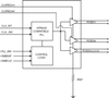

The 9DB106 zero-delay buffer supports PCIe Gen1 and Gen2 clocking requirements. The 9DB106 is driven by a differential SRC output pair from an IDT CK410 / CK505 -compliant main clock generator. It attenuates jitter on the input clock and has a selectable PLL bandwidth to maximize performance in systems with or without Spread-Spectrum clocking. An SMBus interface allows control of the PLL bandwidth and bypass options, while 2 clock request ( CLKREQ #) pins make the 9DB106 suitable for Express Card applications.
| Integrated Device Technology | |
|---|---|
| Product Category | IC Interfaces |
| Product Number | 9DB106BGILF |
| Product Name | 6-output Differential Buffer For PCIe Gen2 |
| Technology | PCI Express |
| Device Type | Buffer |
| Supply Voltage | 3.3V |
| Pd | 429 milliwatts |