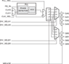

The 8752I is a low voltage, low skew LVCMOS clock generator. With output up to 240MHz, the 8752I is targeted for high performance clock applications. Along with a fully integrated PLL , the 8752I contains frequency configurable outputs and an external feedback input for regenerating clocks with "zero delay".
Dual clock inputs, CLK0 and CLK1 , support redundant clock applications. The CLK_SEL input determines which reference clock is used. The output divider values of Bank A and B are controlled by the DIV_SELA0:1, and DIV_SELB0:1, respectively.
For test and system debug purposes, the PLL_SEL input allows the PLL to be bypassed. When HIGH , the MR /nOE input resets the internal dividers and forces the outputs to the high impedance state.
The low impedance LVCMOS outputs of the 8752I are designed to drive terminated transmission lines. The effective fanout of each output can be doubled by utilizing the ability of each output to drive two series terminated transmission lines.
| Integrated Device Technology | |
|---|---|
| Product Category | IC Interfaces |
| Product Number | 8752CYILFT |
| Product Name | Low Skew, 1-to-8 LVCMOS Clock Multiplier/Zero Delay Buffer |
| Technology | CMOS |
| Device Type | Buffer |
| Supply Voltage | 2.5V; 3.3V |