Integrated Device Technology 175MHz,FemtoClock VCXO Based SONET/SDH Jitter Attenuator 843002AKI-40LFT

Description
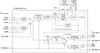
The 843002I-40 is a PLL based synchronous clock generator that is optimized for SONET / SDH line card applications where jitter attenuation and frequency translation is needed. The device contains two internal PLL stages that are cascaded in series. The first PLL stage uses a VCXO which is optimized to provide reference clock jitter attenuation and to be jitter tolerant, and to provide a stable reference clock for the 2nd PLL stage (typically 19.44MHz). The second PLL stage provides additional frequency multiplication (x32), and it maintains low output jitter by using a low phase noise FemtoClock VCO . PLL multiplication ratios are selected from internal lookup tables using device input selection pins. The device performance and the PLL multiplication ratios are optimized to support non- FEC (non-Forward Error Correction) SONET / SDH applications with rates up to OC -48 ( SONET ) or STM -16 ( SDH ). The VCXO requires the use of an external, inexpensive pullable crystal. VCXO PLL uses external passive loop filter components which are used to optimize the PLL loop bandwidth and damping characteristics for the given line card application. The 843002I-40 includes two clock input ports. Each one can accept either a single-ended or differential input. Each input port also includes an activity detector circuit, which reports input clock activity through the LOR0 and LOR1 logic output pins. The two input ports feed an input selection mux. "Hitless switching" is accomplished through proper filter tuning. Jitter transfer and wander characteristics are influenced by loop filter tuning, and phase transient performance is influenced by both loop filter tuning and alignment error between the two reference clocks. Typical 843002I-40 configuration in SONET / SDH Systems: VCXO 19.44MHz crystal Input Reference clock frequency selections: 19.44MHz, 38.88MHz, 77.76MHz, 155.52MHz, 311.04MHz, 622.08MHz Output clock frequency selections: 19.44MHz, 77.76MHz, 155.52MHz, Hi-Z
Datasheet
Description
The 843002I-40 is a PLL based synchronous clock generator that is optimized for SONET / SDH line card applications where jitter attenuation and frequency translation is needed. The device contains two internal PLL stages that are cascaded in series. The first PLL stage uses a VCXO which is optimized to provide reference clock jitter attenuation and to be jitter tolerant, and to provide a stable reference clock for the 2nd PLL stage (typically 19.44MHz). The second PLL stage provides additional frequency multiplication (x32), and it maintains low output jitter by using a low phase noise FemtoClock VCO . PLL multiplication ratios are selected from internal lookup tables using device input selection pins. The device performance and the PLL multiplication ratios are optimized to support non- FEC (non-Forward Error Correction) SONET / SDH applications with rates up to OC -48 ( SONET ) or STM -16 ( SDH ). The VCXO requires the use of an external, inexpensive pullable crystal. VCXO PLL uses external passive loop filter components which are used to optimize the PLL loop bandwidth and damping characteristics for the given line card application. The 843002I-40 includes two clock input ports. Each one can accept either a single-ended or differential input. Each input port also includes an activity detector circuit, which reports input clock activity through the LOR0 and LOR1 logic output pins. The two input ports feed an input selection mux. "Hitless switching" is accomplished through proper filter tuning. Jitter transfer and wander characteristics are influenced by loop filter tuning, and phase transient performance is influenced by both loop filter tuning and alignment error between the two reference clocks. Typical 843002I-40 configuration in SONET / SDH Systems: VCXO 19.44MHz crystal Input Reference clock frequency selections: 19.44MHz, 38.88MHz, 77.76MHz, 155.52MHz, 311.04MHz, 622.08MHz Output clock frequency selections: 19.44MHz, 77.76MHz, 155.52MHz, Hi-Z
Datasheet

Suppliers

Company
Product
Description
Supplier Links
175MHz,FemtoClock VCXO Based SONET/SDH Jitter Attenuator - 843002AKI-40LFT - Integrated Device Technology
San Jose, CA, USA
175MHz,FemtoClock VCXO Based SONET/SDH Jitter Attenuator
843002AKI-40LFT
175MHz,FemtoClock VCXO Based SONET/SDH Jitter Attenuator 843002AKI-40LFT
The 843002I-40 is a PLL based synchronous clock generator that is optimized for SONET / SDH line card applications where jitter attenuation and frequency translation is needed. The device contains two internal PLL stages that are cascaded in series. The first PLL stage uses a VCXO which is optimized to provide reference clock jitter attenuation and to be jitter tolerant, and to provide a stable reference clock for the 2nd PLL stage (typically 19.44MHz). The second PLL stage provides additional frequency multiplication (x32), and it maintains low output jitter by using a low phase noise FemtoClock VCO . PLL multiplication ratios are selected from internal lookup tables using device input selection pins. The device performance and the PLL multiplication ratios are optimized to support non- FEC (non-Forward Error Correction) SONET / SDH applications with rates up to OC -48 ( SONET ) or STM -16 ( SDH ). The VCXO requires the use of an external, inexpensive pullable crystal. VCXO PLL uses external passive loop filter components which are used to optimize the PLL loop bandwidth and damping characteristics for the given line card application. The 843002I-40 includes two clock input ports. Each one can accept either a single-ended or differential input. Each input port also includes an activity detector circuit, which reports input clock activity through the LOR0 and LOR1 logic output pins. The two input ports feed an input selection mux. "Hitless switching" is accomplished through proper filter tuning. Jitter transfer and wander characteristics are influenced by loop filter tuning, and phase transient performance is influenced by both loop filter tuning and alignment error between the two reference clocks. Typical 843002I-40 configuration in SONET / SDH Systems: VCXO 19.44MHz crystal Input Reference clock frequency selections: 19.44MHz, 38.88MHz, 77.76MHz, 155.52MHz, 311.04MHz, 622.08MHz Output clock frequency selections: 19.44MHz, 77.76MHz, 155.52MHz, Hi-Z

The 843002I-40 is a PLL based synchronous clock generator that is optimized for SONET / SDH line card applications where jitter attenuation and frequency translation is needed. The device contains two internal PLL stages that are cascaded in series. The first PLL stage uses a VCXO which is optimized to provide reference clock jitter attenuation and to be jitter tolerant, and to provide a stable reference clock for the 2nd PLL stage (typically 19.44MHz). The second PLL stage provides additional frequency multiplication (x32), and it maintains low output jitter by using a low phase noise FemtoClock VCO . PLL multiplication ratios are selected from internal lookup tables using device input selection pins. The device performance and the PLL multiplication ratios are optimized to support non- FEC (non-Forward Error Correction) SONET / SDH applications with rates up to OC -48 ( SONET ) or STM -16 ( SDH ). The VCXO requires the use of an external, inexpensive pullable crystal. VCXO PLL uses external passive loop filter components which are used to optimize the PLL loop bandwidth and damping characteristics for the given line card application. The 843002I-40 includes two clock input ports. Each one can accept either a single-ended or differential input. Each input port also includes an activity detector circuit, which reports input clock activity through the LOR0 and LOR1 logic output pins. The two input ports feed an input selection mux. "Hitless switching" is accomplished through proper filter tuning. Jitter transfer and wander characteristics are influenced by loop filter tuning, and phase transient performance is influenced by both loop filter tuning and alignment error between the two reference clocks. Typical 843002I-40 configuration in SONET / SDH Systems:

  • VCXO 19.44MHz crystal
  • Input Reference clock frequency selections:
    19.44MHz, 38.88MHz, 77.76MHz, 155.52MHz, 311.04MHz, 622.08MHz
  • Output clock frequency selections:
    19.44MHz, 77.76MHz, 155.52MHz, Hi-Z
Supplier's Site Datasheet

Technical Specifications

  Integrated Device Technology
Product Category IC Phase-locked Loops (PLL)
Product Number 843002AKI-40LFT
Product Name 175MHz,FemtoClock VCXO Based SONET/SDH Jitter Attenuator
Bus Interface LVPECL; LVPECL
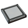
Package Type Surface Mount; VFQFPN
Supply Voltage 3.3 volts
Unlock Full Specs
to access all available technical data

Similar Products

CDC2536 3.3V PLL Clock Driver with 1/2x, 1x and 2x Frequency Options - CDC2536DBR - Texas Instruments
Specs
Package Type SSOP
Supply Voltage 3.3 volts
Frequency 100 MHz
View Details
8 suppliers
Phase-locked loop - HEF4046BT-Q100J - Nexperia B.V.
Specs
Package Type SOT109-1
View Details
2 suppliers
Clock/Timing - Clock/Timing - Clock Generators, PLLs, Frequency Synthesizers - SI5326C-C-GMR - 894644-SI5326C-C-GMR - Win Source Electronics
Specs
Package Type Surface Mount; 36-QFN (6x6)
Operating Temperature -40 to 85 C (-40 to 185 F)
View Details
6 suppliers