Integrated Device Technology 2.5V to 3.3V High Performance Clock Buffer 5V2305NRGI

Description
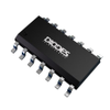
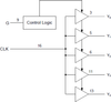
The IDT5V2305 is a high performance, low skew clock buffer that operates up to 200MHz. One bank of five outputs provides low skew copies of CLK . Through the use of control pin G, the outputs of bank Y(0:4) can be placed in a low state regardless of CLK input. The device operates in 2.5V and 3.3V environments. The built-in output enable glitch suppression ensures a synchronized output enable sequence to distribute full period clock signals. The IDT5V2305 is characterized for operation from -40°C to +85°C.
Datasheet
Description
The IDT5V2305 is a high performance, low skew clock buffer that operates up to 200MHz. One bank of five outputs provides low skew copies of CLK . Through the use of control pin G, the outputs of bank Y(0:4) can be placed in a low state regardless of CLK input. The device operates in 2.5V and 3.3V environments. The built-in output enable glitch suppression ensures a synchronized output enable sequence to distribute full period clock signals. The IDT5V2305 is characterized for operation from -40°C to +85°C.
Datasheet

Suppliers

Company
Product
Description
Supplier Links
2.5V to 3.3V High Performance Clock Buffer - 5V2305NRGI - Integrated Device Technology
San Jose, CA, USA
2.5V to 3.3V High Performance Clock Buffer
5V2305NRGI
2.5V to 3.3V High Performance Clock Buffer 5V2305NRGI
The IDT5V2305 is a high performance, low skew clock buffer that operates up to 200MHz. One bank of five outputs provides low skew copies of CLK . Through the use of control pin G, the outputs of bank Y(0:4) can be placed in a low state regardless of CLK input. The device operates in 2.5V and 3.3V environments. The built-in output enable glitch suppression ensures a synchronized output enable sequence to distribute full period clock signals. The IDT5V2305 is characterized for operation from -40°C to +85°C.

The IDT5V2305 is a high performance, low skew clock buffer that operates up to 200MHz. One bank of five outputs provides low skew copies of CLK . Through the use of control pin G, the outputs of bank Y(0:4) can be placed in a low state regardless of CLK input. The device operates in 2.5V and 3.3V environments. The built-in output enable glitch suppression ensures a synchronized output enable sequence to distribute full period clock signals. The IDT5V2305 is characterized for operation from -40°C to +85°C.

Supplier's Site Datasheet

Technical Specifications

  Integrated Device Technology
Product Category IC Interfaces
Product Number 5V2305NRGI
Product Name 2.5V to 3.3V High Performance Clock Buffer
Device Type Buffer
Unlock Full Specs
to access all available technical data

Similar Products

Specs
Device Type Laser Driver
Features RoHS
Supply Voltage 3.3V
View Details
Type 38.21 - Timed interface modules - EMR & SSR - 382101258240 - Finder S.p.A. con unico socio
Specs
Device Type Sensor Interface
View Details
Hex inverting Schmitt trigger - 74ALVC14BQ,115 - Nexperia B.V.
Specs
Technology TTL
Features RoHS
Supply Voltage 1.8V; 2.5V; 2.7V; 3V; 3.3V; 3.6V; Other; 1.65 - 3.6
View Details
Driver Ic; Supply Voltage Min Allegro Microsystems - 01F263 - Newark, An Avnet Company
Specs
Supply Voltage Other; 4.5V
# of Devices 1 #
View Details