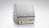
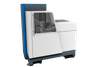
The models of the XDV® range are the most powerful X-ray fluorescence instruments in the Fischer portfolio. They are equipped with a highly sensitive silicon drift detector (SDD) as well as a micro-focus tube; they can further be fitted with different apertures and filters. This makes them ideal for very demanding measurement tasks. Using XDV devices you can, for instance, analyze the thickness and elemental composition of coatings just 5 nm thick and test structures of just 10 µm.
Features
Precise measurement of the thinnest coatings with repeatable accuracy, thanks to high-performance X-ray tubes and sensitive silicon drift detectors (SDD)
Extremely robust construction for long-lasting serial testing, with outstanding long-term stability
Advanced polycapillary X-ray optics to focus the X-rays on an extremely small measurement surface
Automated serial testing with programmable XY-table and Z-axis (optional)
Fast and simple positioning of the probes with the help of video imaging and laser pointer
Applications:
Coating Thickness Measurement
Anti-wear coatings such as NiP layers on the tiniest of watch components
Very thin precious-metal coatings on visible components in mechanical watch movements
Testing base metallization layers (Under Bump Metallization, UBM) in the nanometer range
Measurement of C4 and smaller solder bumps
Material Analysis
Detection of undesirable substances (for example heavy metals) in electronics, packaging and consumer goods according to RoHS, WEEE, CPSIA and other guidelines
Composition of functional coatings, such as the determination of phosphorous content in NiP
Analysis of gold and other precious metals, as well as alloys thereof
Analysis of lead-free solder caps on copper pillars
Testing the elemental composition of C4 and smaller solder bumps, base metallization layers (UBM) and small contact surfaces in the semiconductor industry
The models of the XDV® range are the most powerful X-ray fluorescence instruments in the Fischer portfolio. They are equipped with a highly sensitive silicon drift detector (SDD) as well as a micro-focus tube; they can further be fitted with different apertures and filters. This makes them ideal for very demanding measurement tasks. Using XDV devices you can, for instance, analyze the thickness and elemental composition of coatings just 5 nm thick and test structures of just 10 µm.
Features
- Precise measurement of the thinnest coatings with repeatable accuracy, thanks to high-performance X-ray tubes and sensitive silicon drift detectors (SDD)
- Extremely robust construction for long-lasting serial testing, with outstanding long-term stability
- Advanced polycapillary X-ray optics to focus the X-rays on an extremely small measurement surface
- Automated serial testing with programmable XY-table and Z-axis (optional)
- Fast and simple positioning of the probes with the help of video imaging and laser pointer
Applications:
Coating Thickness Measurement
- Anti-wear coatings such as NiP layers on the tiniest of watch components
- Very thin precious-metal coatings on visible components in mechanical watch movements
- Testing base metallization layers (Under Bump Metallization, UBM) in the nanometer range
- Measurement of C4 and smaller solder bumps
Material Analysis
- Detection of undesirable substances (for example heavy metals) in electronics, packaging and consumer goods according to RoHS, WEEE, CPSIA and other guidelines
- Composition of functional coatings, such as the determination of phosphorous content in NiP
- Analysis of gold and other precious metals, as well as alloys thereof
- Analysis of lead-free solder caps on copper pillars
- Testing the elemental composition of C4 and smaller solder bumps, base metallization layers (UBM) and small contact surfaces in the semiconductor industry