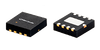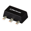
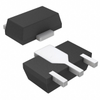
Mini-Circuits SMT MMIC, Medium Power, Linear, HBT Amplifier, DC to 7000 MHz, 50Ω, SOT-89 Style Package GVA-84+

Description
GVA-84+ (RoHS compliant) is a wideband amplifier offering high dynamic range. Lead finish is SnAgNi. It has repeatable performance from lot to lot and is enclosed in a SOT-89 package. It uses patented Transient Protected Darlington configuration and is fabricated using InGaP HBT technology. SIMPLIFIED SCHEMATIC AND PIN DESCRIPTION RF-OUT and DC-IN RF-IN 3 RF-OUT & DC-IN 4 2 GROUND 1 RF-IN GROUND Pin Function Description Number RF-IN 1 RF input pin. This pin requires the use of an external DC blocking capacitor chosen for the frequency of operation. RF-OUT RF output and bias pin. DC voltage is present on this pin; therefore a DC blocking capacitor is necessary for proper operation. An RF choke 3 and DC-IN is needed to feed DC bias without loss of RF signal due to the bias connection, as shown in “Recommended Application Circuit”, Fig. 2 Connections to ground. Use via holes as shown in “Suggested Layout for PCB Design” to reduce ground path inductance for best GND 2,4 performance. REV. E ECO-010314 GVA-84+ MCL NY 240801 www.minicircuits.com P.O. Box 350166, Brooklyn, NY 11235-0003 (718) 934-4500 sales@minicircuits.c om PAGE 1 OF 1 +5 VOLT SURFACE MOUNT Monolithic Amplifier GVA-84+ 50Ω DC to 7 GHz
Request a Quote
Description
GVA-84+ (RoHS compliant) is a wideband amplifier offering high dynamic range. Lead finish is SnAgNi. It has repeatable performance from lot to lot and is enclosed in a SOT-89 package. It uses patented Transient Protected Darlington configuration and is fabricated using InGaP HBT technology. SIMPLIFIED SCHEMATIC AND PIN DESCRIPTION RF-OUT and DC-IN RF-IN 3 RF-OUT & DC-IN 4 2 GROUND 1 RF-IN GROUND Pin Function Description Number RF-IN 1 RF input pin. This pin requires the use of an external DC blocking capacitor chosen for the frequency of operation. RF-OUT RF output and bias pin. DC voltage is present on this pin; therefore a DC blocking capacitor is necessary for proper operation. An RF choke 3 and DC-IN is needed to feed DC bias without loss of RF signal due to the bias connection, as shown in “Recommended Application Circuit”, Fig. 2 Connections to ground. Use via holes as shown in “Suggested Layout for PCB Design” to reduce ground path inductance for best GND 2,4 performance. REV. E ECO-010314 GVA-84+ MCL NY 240801 www.minicircuits.com P.O. Box 350166, Brooklyn, NY 11235-0003 (718) 934-4500 sales@minicircuits.c om PAGE 1 OF 1 +5 VOLT SURFACE MOUNT Monolithic Amplifier GVA-84+ 50Ω DC to 7 GHz
Request a Quote
Datasheet
Datasheet Summary
Powered by GS/AI

GVA-84+ is a +5 V surface mount monolithic amplifier with a frequency range of DC to 7 GHz, designed for high dynamic range applications in base station infrastructure, portable wireless, and LTE systems. It is housed in an SOT-89 package with case style DF782, and features an exposed paddle for thermal management. The amplifier provides typ. gain of 24 dB at 100 MHz, output P1dB of +20.5 dBm, and output IP3 of +37 dBm at 100 MHz. It operates with a supply voltage of +5 V, draws 108 mA typical current, and maintains unconditionally stable performance with transient protection. The device is rated for operation from -45°C to +85°C, has MSL1 moisture sensitivity, and meets HBM ESD Class 1C (1000V to <2000V) and MM ESD Class M2 (100V to <200V). Lead finish is SnAgNi, and it is RoHS compliant.

Datasheet Summary
Powered by GS/AI

GVA-84+ is a +5 V surface mount monolithic amplifier with a frequency range of DC to 7 GHz, designed for high dynamic range applications in base station infrastructure, portable wireless, and LTE systems. It is housed in an SOT-89 package with case style DF782, and features an exposed paddle for thermal management. The amplifier provides typ. gain of 24 dB at 100 MHz, output P1dB of +20.5 dBm, and output IP3 of +37 dBm at 100 MHz. It operates with a supply voltage of +5 V, draws 108 mA typical current, and maintains unconditionally stable performance with transient protection. The device is rated for operation from -45°C to +85°C, has MSL1 moisture sensitivity, and meets HBM ESD Class 1C (1000V to <2000V) and MM ESD Class M2 (100V to <200V). Lead finish is SnAgNi, and it is RoHS compliant.

Suppliers

Company
Product
Description
Supplier Links
SMT MMIC, Medium Power, Linear, HBT Amplifier, DC to 7000 MHz, 50Ω, SOT-89 Style Package - GVA-84+ - Mini-Circuits
Brooklyn, NY, United States
SMT MMIC, Medium Power, Linear, HBT Amplifier, DC to 7000 MHz, 50Ω, SOT-89 Style Package
GVA-84+
SMT MMIC, Medium Power, Linear, HBT Amplifier, DC to 7000 MHz, 50Ω, SOT-89 Style Package GVA-84+
GVA-84+ (RoHS compliant) is a wideband amplifier offering high dynamic range. Lead finish is SnAgNi. It has repeatable performance from lot to lot and is enclosed in a SOT-89 package. It uses patented Transient Protected Darlington configuration and is fabricated using InGaP HBT technology. SIMPLIFIED SCHEMATIC AND PIN DESCRIPTION RF-OUT and DC-IN RF-IN 3 RF-OUT & DC-IN 4 2 GROUND 1 RF-IN GROUND Pin Function Description Number RF-IN 1 RF input pin. This pin requires the use of an external DC blocking capacitor chosen for the frequency of operation. RF-OUT RF output and bias pin. DC voltage is present on this pin; therefore a DC blocking capacitor is necessary for proper operation. An RF choke 3 and DC-IN is needed to feed DC bias without loss of RF signal due to the bias connection, as shown in “Recommended Application Circuit”, Fig. 2 Connections to ground. Use via holes as shown in “Suggested Layout for PCB Design” to reduce ground path inductance for best GND 2,4 performance. REV. E ECO-010314 GVA-84+ MCL NY 240801 www.minicircuits.com P.O. Box 350166, Brooklyn, NY 11235-0003 (718) 934-4500 sales@minicircuits.c om PAGE 1 OF 1 +5 VOLT SURFACE MOUNT Monolithic Amplifier GVA-84+ 50Ω DC to 7 GHz

GVA-84+ (RoHS compliant) is a wideband amplifier offering high dynamic range. Lead finish is SnAgNi. It has repeatable performance from lot to lot and is enclosed in a SOT-89 package. It uses patented Transient Protected Darlington configuration and is fabricated using InGaP HBT technology. SIMPLIFIED SCHEMATIC AND PIN DESCRIPTION RF-OUT and DC-IN RF-IN 3 RF-OUT & DC-IN 4 2 GROUND 1 RF-IN GROUND Pin Function Description Number RF-IN 1 RF input pin. This pin requires the use of an external DC blocking capacitor chosen for the frequency of operation. RF-OUT RF output and bias pin. DC voltage is present on this pin; therefore a DC blocking capacitor is necessary for proper operation. An RF choke 3 and DC-IN is needed to feed DC bias without loss of RF signal due to the bias connection, as shown in “Recommended Application Circuit”, Fig. 2 Connections to ground. Use via holes as shown in “Suggested Layout for PCB Design” to reduce ground path inductance for best GND 2,4 performance. REV. E ECO-010314 GVA-84+ MCL NY 240801 www.minicircuits.com P.O. Box 350166, Brooklyn, NY 11235-0003 (718) 934-4500 sales@minicircuits.com PAGE 1 OF 1 +5 VOLT SURFACE MOUNT Monolithic Amplifier GVA-84+ 50Ω DC to 7 GHz

Supplier's Site Datasheet
Laguna Hills, CA, United States
RF Amplifiers - GVA-84+
1178081-GVA-84+
RF Amplifiers - GVA-84+ 1178081-GVA-84+
Manufacturer: Mini-Circuits Win Source Part Number: 1178081-GVA-84+ Manufacturer Homepage: www.minicircuits.com RoHS State: Request Verification Is this a common-used part?: Yes Popularity: High Fake Threat In the Open Market: 61 pct. Supply and Demand Status: Balance

Manufacturer: Mini-Circuits
Win Source Part Number: 1178081-GVA-84+
Manufacturer Homepage: www.minicircuits.com
RoHS State: Request Verification
Is this a common-used part?: Yes
Popularity: High
Fake Threat In the Open Market: 61 pct.
Supply and Demand Status: Balance

Buy Now
RF Amplifiers - 3157-GVA-84+CT-ND - DigiKey
Thief River Falls, MN, United States
RF Amplifiers
3157-GVA-84+CT-ND
RF Amplifiers 3157-GVA-84+CT-ND
RF Amplifier IC CATV, DBS, LTE, MMDS, Wireless LAN 0Hz ~ 7GHz SOT-89

RF Amplifier IC CATV, DBS, LTE, MMDS, Wireless LAN 0Hz ~ 7GHz SOT-89

Buy Now Datasheet
RF Amplifiers - 3157-GVA-84+TR-ND - DigiKey
Thief River Falls, MN, United States
RF Amplifiers
3157-GVA-84+TR-ND
RF Amplifiers 3157-GVA-84+TR-ND
RF Amplifier IC CATV, DBS, LTE, MMDS, Wireless LAN 0Hz ~ 7GHz SOT-89

RF Amplifier IC CATV, DBS, LTE, MMDS, Wireless LAN 0Hz ~ 7GHz SOT-89

Buy Now Datasheet
RF Amplifiers - 3157-GVA-84+DKR-ND - DigiKey
Thief River Falls, MN, United States
RF Amplifiers
3157-GVA-84+DKR-ND
RF Amplifiers 3157-GVA-84+DKR-ND
RF Amplifier IC CATV, DBS, LTE, MMDS, Wireless LAN 0Hz ~ 7GHz SOT-89

RF Amplifier IC CATV, DBS, LTE, MMDS, Wireless LAN 0Hz ~ 7GHz SOT-89

Buy Now Datasheet

Technical Specifications

  Mini-Circuits Win Source Electronics DigiKey
Product Category RF Amplifiers RF Amplifiers RF Amplifiers
Product Number GVA-84+ 1178081-GVA-84+ 3157-GVA-84+CT-ND
Product Name SMT MMIC, Medium Power, Linear, HBT Amplifier, DC to 7000 MHz, 50Ω, SOT-89 Style Package RF Amplifiers - GVA-84+ RF Amplifiers
Amplifier Type Power Amplifier Low Noise Amplifier; Power Amplifier
RoHS Compliant RoHS
Frequency Range 7000 MHz 0.0 to 7000 MHz
Minimum Gain 4.00E-4 dB 10.5 dB
Maximum Gain 25.3 dB 10.5 dB
Unlock Full Specs
to access all available technical data

Similar Products

DOCSIS 3.1 MMIC Power Doubler Amplifier, 75Ω, 45 to 1218 MHz - ADCA3270 - Mini-Circuits
Specs
Amplifier Type Power Amplifier
MMIC Tech. MMIC
View Details
SMT MMIC, Medium Power, Linear, Dual Matched, HBT Amplifier, DC to 4000 MHz, 50Ω, QFN Style Package - MERA-533+ - Mini-Circuits
Specs
Amplifier Type Power Amplifier
Operating Temperature -40 to 85 C (-40 to 185 F)
Frequency Range 4000 MHz
View Details
3 suppliers
Specs
Applications RF Microwave
View Details
SMT MMIC, Medium Power pHEMT Amplifier, 6 - 18 GHz, 50Ω, 5x5 mm QFN Style Package - AVA-6183MP+ - Mini-Circuits
Specs
Amplifier Type Power Amplifier
Operating Temperature -55 to 85 C (-67 to 185 F)
Frequency Range 6000 to 18000 MHz
View Details