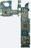
High-density interconnection (HDI) substrates have high-density circuits that make it possible for electronic parts mounted on a PCB to send and recieve electrical signals between themselves.
The products are used for mounting the main parts of mobile devices and transmitting their signals.
General Features
Improves the performance of products because of high integration
Makes it easier to automate the assembly of PCBs
Reduces total costs
Application
Note PC(Cellular Phone, Tablet, DSC, Game Consol)
IC Module, Main Board
Why Samsung
The products allow transmission of signals at high speeds by making PCBs smaller and shortening the signal path.
Features
SAVIA is a product that has stack vias formed in all layers. Stack vias are formed through fill plating and have superb performance in terms of transmission and reflection than staggered vias.
Slim PCB
Stiffness is enhanced by using thin materials with high coefficient of elasticity. Electric signal characteristics are excellent as materials of low permitivity are used.
High Stiffness
Stiffness is increased by applying materials with high coefficient of elasticity, and thereby improving the quality of partsmounting through the enhanced flex characteristics of slim PCBs (60 ㎛ CCL, 40/50 ㎛ Prepreg).
Impedance Matching
Electric signal characteristics are excellent as microcircuits and materials of low Dk (low permitivity) are applied.
UHD(Ultra High Density) PCB
UHD PCBs can be made in a high-density design, thanks to microcircuits and microholes.
Design Rule
0.35 ㎜P 1Trace (Via/Land : 70/200 ㎛, L/S : 50/50 ㎛)
0.4 ㎜P 2Trace (Via/Land : 70/180 ㎛, L/S : 40/40 ㎛)
0.3 ㎜P (Via/Land : 70/150 ㎛, L/S : 30/30 ㎛)
Core Tech
Registration Alignment 75㎛ → 65 ㎛ → 55 ㎛ → 50 ㎛ → 40 ㎛
Ultra High Density PCB Forming Technology
Cavity Type
Cavity PCBs have step differences in the areas where components are mounted. They allow a reduction in the overall thickness even if a thick component is mounted.
There are two types of cavity: the non-component type which cannot mount component inside the cavity. and the component type which can mount components due to the formation of Sralc Pad.
Non Component Type
Reducing thickness of specific area
High Volume Manufacturing
Depth : ~ 400 ㎛
Application Wearable Device
Component Type
Reduce the thickness of an assembled device ※ HDI desing rules remain the same (0.4 Pitch)
Under Developing
Depth : ~ 250 ㎛
Application - Smart Phone - Tablet PC / Note PC
Pad type
Realizes SMD PAD and NSMD PAD
adsizes are created based on each pitch according to the mounting methods and the needs of customers - SMD : Solder Mask Defined - NSMD : Non Solder Mask Defined
Technology
- Able to form solder resister in the BGA Pad section - Various materials such as PSR ink, Coverlay, Prepreg and others are used to form the register
Key Core Technologies
Owns HDI/BGA/FCBGA technologies and develops leading technologies through convergence and integration of technologies.
Quality
1) FE-SEM (Field Emission-Scanning Electron Microscope) 2) EDS(Energy Dispersive X-ray Spectroscopy) 3) FT-IR (Fourier Transform-Infra Red Spectrometer) 4) TMA (Thermo Mechanical Analyzer) 5) IMS ( Ion Milling System) 6) TXP (Target X Preparation) 7) FIB (Focused Ion Beam)
High-density interconnection (HDI) substrates have high-density circuits that make it possible for electronic parts mounted on a PCB to send and recieve electrical signals between themselves.
The products are used for mounting the main parts of mobile devices and transmitting their signals.
General Features
- Improves the performance of products because of high integration
- Makes it easier to automate the assembly of PCBs
- Reduces total costs
Application
- Note PC(Cellular Phone, Tablet, DSC, Game Consol)
- IC Module, Main Board
Why Samsung
The products allow transmission of signals at high speeds by making PCBs smaller and shortening the signal path.
Features
SAVIA is a product that has stack vias formed in all layers. Stack vias are formed through fill plating and have superb performance in terms of transmission and reflection than staggered vias.
Slim PCB
Stiffness is enhanced by using thin materials with high coefficient of elasticity. Electric signal characteristics are excellent as materials of low permitivity are used.
High Stiffness
Stiffness is increased by applying materials with high coefficient of elasticity, and thereby improving the quality of partsmounting through the enhanced flex characteristics of slim PCBs (60 ㎛ CCL, 40/50 ㎛ Prepreg).
Impedance Matching
Electric signal characteristics are excellent as microcircuits and materials of low Dk (low permitivity) are applied.
UHD(Ultra High Density) PCB
UHD PCBs can be made in a high-density design, thanks to microcircuits and microholes.
Design Rule
- 0.35 ㎜P 1Trace (Via/Land : 70/200 ㎛, L/S : 50/50 ㎛)
- 0.4 ㎜P 2Trace (Via/Land : 70/180 ㎛, L/S : 40/40 ㎛)
- 0.3 ㎜P (Via/Land : 70/150 ㎛, L/S : 30/30 ㎛)
Core Tech
- Registration Alignment 75㎛ → 65 ㎛ → 55 ㎛ → 50 ㎛ → 40 ㎛
Ultra High Density PCB Forming Technology
Cavity Type
Cavity PCBs have step differences in the areas where components are mounted. They allow a reduction in the overall thickness even if a thick component is mounted.
There are two types of cavity: the non-component type which cannot mount component inside the cavity. and the component type which can mount components due to the formation of Sralc Pad.
Non Component Type
Reducing thickness of specific area
- High Volume Manufacturing
- Depth : ~ 400 ㎛
- Application
Wearable Device
Component Type
Reduce the thickness of an assembled device
※ HDI desing rules remain the same (0.4 Pitch)
- Under Developing
- Depth : ~ 250 ㎛
- Application
- Smart Phone
- Tablet PC / Note PC
Pad type
Realizes SMD PAD and NSMD PAD
adsizes are created based on each pitch according to the mounting methods and the needs of customers
- SMD : Solder Mask Defined
- NSMD : Non Solder Mask Defined
Technology
- Able to form solder resister in the BGA Pad section
- Various materials such as PSR ink, Coverlay, Prepreg and others are used to form the register
Key Core Technologies
Owns HDI/BGA/FCBGA technologies and develops leading technologies through convergence and integration of technologies.
Quality
1) FE-SEM (Field Emission-Scanning Electron Microscope) 2) EDS(Energy Dispersive X-ray Spectroscopy)
3) FT-IR (Fourier Transform-Infra Red Spectrometer) 4) TMA (Thermo Mechanical Analyzer) 5) IMS ( Ion Milling System)
6) TXP (Target X Preparation) 7) FIB (Focused Ion Beam)