Nexperia B.V. Triple inverter with open-drain output 74LVC3G06GN,115

Description
The 74LVC3G06 is a triple inverter with open-drain outputs. Inputs can be driven from either 3.3 V or 5 V devices. This feature allows the use of these devices as translators in mixed 3.3 V and 5 V environments. Schmitt-trigger action at all inputs makes the circuit tolerant of slower input rise and fall times. This device is fully specified for partial power down applications using IOFF. The IOFF circuitry disables the output, preventing the potentially damaging backflow current through the device when it is powered down. Features and benefits Wide supply voltage range from 1.65 V to 5.5 V Overvoltage tolerant inputs to 5.5 V High noise immunity -24 mA output drive (VCC = 3.0 V) CMOS low power consumption Latch-up performance exceeds 250 mA Direct interface with TTL levels IOFF circuitry provides partial Power-down mode operation Complies with JEDEC standard: JESD8-7 (1.65 V to 1.95 V) JESD8-5 (2.3 V to 2.7 V) JESD8-B/JESD36 (2.7 V to 3.6 V) ESD protection: HBM: ANSI/ESDA/JEDEC JS-001 class 2 exceeds 2000 V CDM: ANSI/ESDA/JEDEC JS-002 class C3 exceeds 1000 V Multiple package options Specified from -40 °C to +85 °C and -40 °C to +125 °C
Request a Quote
Description
The 74LVC3G06 is a triple inverter with open-drain outputs. Inputs can be driven from either 3.3 V or 5 V devices. This feature allows the use of these devices as translators in mixed 3.3 V and 5 V environments. Schmitt-trigger action at all inputs makes the circuit tolerant of slower input rise and fall times. This device is fully specified for partial power down applications using IOFF. The IOFF circuitry disables the output, preventing the potentially damaging backflow current through the device when it is powered down. Features and benefits Wide supply voltage range from 1.65 V to 5.5 V Overvoltage tolerant inputs to 5.5 V High noise immunity -24 mA output drive (VCC = 3.0 V) CMOS low power consumption Latch-up performance exceeds 250 mA Direct interface with TTL levels IOFF circuitry provides partial Power-down mode operation Complies with JEDEC standard: JESD8-7 (1.65 V to 1.95 V) JESD8-5 (2.3 V to 2.7 V) JESD8-B/JESD36 (2.7 V to 3.6 V) ESD protection: HBM: ANSI/ESDA/JEDEC JS-001 class 2 exceeds 2000 V CDM: ANSI/ESDA/JEDEC JS-002 class C3 exceeds 1000 V Multiple package options Specified from -40 °C to +85 °C and -40 °C to +125 °C
Request a Quote
Datasheet
Datasheet Summary
Powered by GS/AI

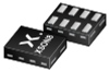
The 74LVC3G06GN is a triple inverter with open-drain outputs designed for mixed-voltage environments, supporting input levels from 1.65 V to 5.5 V. It features Schmitt-trigger inputs for tolerance of slow signal edges and I<sub>OFF</sub> circuitry to prevent backflow current during partial power-down. The device is packaged in an XSON8 no-lead format with a body measuring 1.2 × 1.0 × 0.35 mm, specified for operation from -40 °C to +125 °C. It offers -24 mA output drive at V<sub>CC</sub> = 3.0 V, complies with JEDEC JESD8-7, JESD8-5, and JESD8-B/JESD36 standards, and meets ESD protection ratings of HBM class 2 exceeding 2000 V and CDM class C3 exceeding 1000 V.

Datasheet Summary
Powered by GS/AI

The 74LVC3G06GN is a triple inverter with open-drain outputs designed for mixed-voltage environments, supporting input levels from 1.65 V to 5.5 V. It features Schmitt-trigger inputs for tolerance of slow signal edges and I<sub>OFF</sub> circuitry to prevent backflow current during partial power-down. The device is packaged in an XSON8 no-lead format with a body measuring 1.2 × 1.0 × 0.35 mm, specified for operation from -40 °C to +125 °C. It offers -24 mA output drive at V<sub>CC</sub> = 3.0 V, complies with JEDEC JESD8-7, JESD8-5, and JESD8-B/JESD36 standards, and meets ESD protection ratings of HBM class 2 exceeding 2000 V and CDM class C3 exceeding 1000 V.

Suppliers

Company
Product
Description
Supplier Links
Triple inverter with open-drain output - 74LVC3G06GN,115 - Nexperia B.V.
Nijmegen, Netherlands
Triple inverter with open-drain output
74LVC3G06GN,115
Triple inverter with open-drain output 74LVC3G06GN,115
The 74LVC3G06 is a triple inverter with open-drain outputs. Inputs can be driven from either 3.3 V or 5 V devices. This feature allows the use of these devices as translators in mixed 3.3 V and 5 V environments. Schmitt-trigger action at all inputs makes the circuit tolerant of slower input rise and fall times. This device is fully specified for partial power down applications using IOFF. The IOFF circuitry disables the output, preventing the potentially damaging backflow current through the device when it is powered down. Features and benefits Wide supply voltage range from 1.65 V to 5.5 V Overvoltage tolerant inputs to 5.5 V High noise immunity -24 mA output drive (VCC = 3.0 V) CMOS low power consumption Latch-up performance exceeds 250 mA Direct interface with TTL levels IOFF circuitry provides partial Power-down mode operation Complies with JEDEC standard: JESD8-7 (1.65 V to 1.95 V) JESD8-5 (2.3 V to 2.7 V) JESD8-B/JESD36 (2.7 V to 3.6 V) ESD protection: HBM: ANSI/ESDA/JEDEC JS-001 class 2 exceeds 2000 V CDM: ANSI/ESDA/JEDEC JS-002 class C3 exceeds 1000 V Multiple package options Specified from -40 °C to +85 °C and -40 °C to +125 °C

The 74LVC3G06 is a triple inverter with open-drain outputs. Inputs can be driven from either 3.3 V or 5 V devices. This feature allows the use of these devices as translators in mixed 3.3 V and 5 V environments.

Schmitt-trigger action at all inputs makes the circuit tolerant of slower input rise and fall times.

This device is fully specified for partial power down applications using IOFF. The IOFF circuitry disables the output, preventing the potentially damaging backflow current through the device when it is powered down.

Features and benefits

  • Wide supply voltage range from 1.65 V to 5.5 V
  • Overvoltage tolerant inputs to 5.5 V
  • High noise immunity
  • -24 mA output drive (VCC = 3.0 V)
  • CMOS low power consumption
  • Latch-up performance exceeds 250 mA
  • Direct interface with TTL levels
  • IOFF circuitry provides partial Power-down mode operation
  • Complies with JEDEC standard:
    • JESD8-7 (1.65 V to 1.95 V)
    • JESD8-5 (2.3 V to 2.7 V)
    • JESD8-B/JESD36 (2.7 V to 3.6 V)
  • ESD protection:
    • HBM: ANSI/ESDA/JEDEC JS-001 class 2 exceeds 2000 V
    • CDM: ANSI/ESDA/JEDEC JS-002 class C3 exceeds 1000 V
  • Multiple package options
  • Specified from -40 °C to +85 °C and -40 °C to +125 °C
Supplier's Site Datasheet
 - 74LVC3G06GN,115 - Rochester Electronics
Newburyport, MA, United States
Inverter, LVC/LCX/Z Series, 3-Func, 1-Input, CMOS, PDSO8

Inverter, LVC/LCX/Z Series, 3-Func, 1-Input, CMOS, PDSO8

Supplier's Site Datasheet

Technical Specifications

  Nexperia B.V. Rochester Electronics
Product Category IC Interfaces IC Interfaces
Product Number 74LVC3G06GN,115 74LVC3G06GN,115
Product Name Triple inverter with open-drain output
Features RoHS RoHS
Unlock Full Specs
to access all available technical data

Similar Products

 - 74AHC244D,112 - Rochester Electronics
Nexperia B.V.
Specs
Device Type Line / Bus Driver
Features RoHS
Package Type SO20
View Details
Bus buffer/line driver; 3-state - 74AHCT1G125GV,125 - Nexperia B.V.
Specs
Device Type Buffer
Features RoHS
Supply Voltage Other; +7.0
View Details
4 suppliers
 - 74ABT126DB,118 - Rochester Electronics
Nexperia B.V.
Specs
Device Type Line / Bus Driver
Features RoHS
Package Type SOP; SSOP; SSOP14
View Details
 - 74ALVC16244DGG,112 - Rochester Electronics
Specs
Device Type Line / Bus Driver
Features RoHS
Package Type SOP; SSOP; TSSOP; TSSOP48
View Details