MicroSense, LLC SigmaTech Wafer Metrology Systems UltraMap-APBP

Description
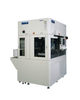
Automated Thickness measurement system Cassette to cassette or manual loading. Patented sensing technology with APBP (dual automated positioning backpressure probes). Manual Loading 20mm resolution Wafer 2" to 12" (50 to 300mm) round or square Thickness range: 200um to 5mm Automated calibration 2D & 3D mapping capability SECS/GEM communication Options Extended warp/bow range up to 5000um Wafer prealigner Samples with special shape (square, rectangle, round) Applications Thickness and shape measurement of wafers made of special materials: ceramics, rough material, plastics, glass, packaging material. Extremely high warp/bow wafers (10mm range).
Description
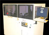
Automated Thickness measurement system Cassette to cassette or manual loading. Patented sensing technology with APBP (dual automated positioning backpressure probes). Manual Loading 20mm resolution Wafer 2" to 12" (50 to 300mm) round or square Thickness range: 200um to 5mm Automated calibration 2D & 3D mapping capability SECS/GEM communication Options Extended warp/bow range up to 5000um Wafer prealigner Samples with special shape (square, rectangle, round) Applications Thickness and shape measurement of wafers made of special materials: ceramics, rough material, plastics, glass, packaging material. Extremely high warp/bow wafers (10mm range).

Suppliers

Company
Product
Description
Supplier Links
SigmaTech Wafer Metrology Systems - UltraMap-APBP - MicroSense, LLC
Lowell, MA, USA
SigmaTech Wafer Metrology Systems
UltraMap-APBP
SigmaTech Wafer Metrology Systems UltraMap-APBP
Automated Thickness measurement system Cassette to cassette or manual loading. Patented sensing technology with APBP (dual automated positioning backpressure probes). Manual Loading 20mm resolution Wafer 2" to 12" (50 to 300mm) round or square Thickness range: 200um to 5mm Automated calibration 2D & 3D mapping capability SECS/GEM communication Options Extended warp/bow range up to 5000um Wafer prealigner Samples with special shape (square, rectangle, round) Applications Thickness and shape measurement of wafers made of special materials: ceramics, rough material, plastics, glass, packaging material. Extremely high warp/bow wafers (10mm range).

Automated Thickness measurement system

Cassette to cassette or manual loading. Patented sensing technology with APBP (dual automated positioning backpressure probes).

Manual Loading

  • 20mm resolution
  • Wafer 2" to 12" (50 to 300mm) round or square
  • Thickness range: 200um to 5mm
  • Automated calibration
  • 2D & 3D mapping capability
  • SECS/GEM communication

Options

  • Extended warp/bow range up to 5000um
  • Wafer prealigner
  • Samples with special shape (square, rectangle, round)

Applications

Thickness and shape measurement of wafers made of special materials: ceramics, rough material, plastics, glass, packaging material. Extremely high warp/bow wafers (10mm range).

Supplier's Site

Technical Specifications

  MicroSense, LLC
Product Category Wafer and Thin Film Instrumentation
Product Number UltraMap-APBP
Product Name SigmaTech Wafer Metrology Systems
Form Factor Monitor or instrument
Mounting / Loading Floor
Technology Automated Positioning Backpressure Probe (APBP)
Unlock Full Specs
to access all available technical data

Similar Products

Wafer UHV Pro - m2-wafer-uhv-pro - Cosmic Equipment SpA
Specs
Form Factor Monitor or instrument
Applications Wafer
View Details
Wafer Edge Grinders - WBM-3000 Series - Daitron Co., Ltd.
Specs
Form Factor Monitor or instrument
Mounting / Loading Floor
Applications Wafer
View Details
EC-52000IC ION CLEANER -  - JEOL USA, Inc.
Specs
Form Factor Monitor or instrument
Mounting / Loading Floor
View Details
MerMaid -  - Imego
Specs
Form Factor ProbingSystem; Sensor or sensing element
Mounting / Loading In-process, in-situ or system mounted; Floor
Technology Quartz crystal microbalance; Magnetoelastic Resonance Sensors (MER)
View Details