The SST25VF080B devices are enhanced with improved operating frequency for lower power consumption. SST25VF080B SPI serial flash memories are manufactured with SST's proprietary, high-performance CMOS SuperFlash technology. The split-gate cell design and thick-oxide tunneling injector attain better reliability and manufacturability compared with alternate approaches.
Additional Features
Single Voltage Read and Write Operations– 2.7-3.6V
Serial Interface Architecture
Supports 50 MHz SPI clock (80 MHz no longer available see EOL NOTIFICATION)
Superior Reliability
Endurance: 100,000 Cycles (typical)
Greater than 100 years Data Retention
Low Power Consumption:
Program & Erase Current: 30mA (max)
Active Read Current: 10 mA (typical)
Standby Current: 5 µA (typical)
Flexible Erase Capability
Uniform 4 KByte sectors
Uniform 32 KByte & 64 KByte overlay blocks
Fast Erase and Byte-Program:
Chip-Erase Time: 35 ms (typical)
Sector-/Block-Erase Time: 18 ms (typical)
Byte-Program Time: 7 µs (typical)
Auto Address Increment (AAI) Programming
Decrease total chip programming time over Byte-Program operations
End-of-Write Detection
Software polling the BUSY bit in Status Register
Busy Status readout on SO pin in AAI Mode
Hold Pin (HOLD#)
Suspends a serial sequence to the memory without deselecting the device
Write Protection (WP#)
Enables/Disables the Lock-Down function of the status register
Software Write Protection
Write protection through Block-Protection bits in the status register
Temperature Range
Commercial: 0°C to +70°C
Industrial: -40°C to +85°C
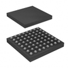
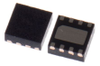
Packages Available– 8-lead SOIC (200 mils)– 8-contact WSON (6mm x 5mm)– 8-lead PDIP (300 mils)– 8-bump CSP
All devices are RoHS compliant
The SST25VF080B devices are enhanced with improved operating frequency for lower power consumption. SST25VF080B SPI serial flash memories are manufactured with SST's proprietary, high-performance CMOS SuperFlash technology. The split-gate cell design and thick-oxide tunneling injector attain better reliability and manufacturability compared with alternate approaches.
Additional Features
- Single Voltage Read and Write Operations– 2.7-3.6V
- Serial Interface Architecture
- Supports 50 MHz SPI clock (80 MHz no longer available see EOL NOTIFICATION)
- Superior Reliability
- Endurance: 100,000 Cycles (typical)
- Greater than 100 years Data Retention
- Low Power Consumption:
- Program & Erase Current: 30mA (max)
- Active Read Current: 10 mA (typical)
- Standby Current: 5 µA (typical)
- Flexible Erase Capability
- Uniform 4 KByte sectors
- Uniform 32 KByte & 64 KByte overlay blocks
- Fast Erase and Byte-Program:
- Chip-Erase Time: 35 ms (typical)
- Sector-/Block-Erase Time: 18 ms (typical)
- Byte-Program Time: 7 µs (typical)
- Auto Address Increment (AAI) Programming
- Decrease total chip programming time over Byte-Program operations
- End-of-Write Detection
- Software polling the BUSY bit in Status Register
- Busy Status readout on SO pin in AAI Mode
- Hold Pin (HOLD#)
- Suspends a serial sequence to the memory without deselecting the device
- Write Protection (WP#)
- Enables/Disables the Lock-Down function of the status register
- Software Write Protection
- Write protection through Block-Protection bits in the status register
- Temperature Range
- Commercial: 0°C to +70°C
- Industrial: -40°C to +85°C
- Packages Available– 8-lead SOIC (200 mils)– 8-contact WSON (6mm x 5mm)– 8-lead PDIP (300 mils)– 8-bump CSP
- All devices are RoHS compliant