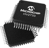
Microchip Technology, Inc. 16-Channel Low Harmonic Distortion High Voltage Analog Switch HV2733

Description
HV2733 is a low charge injection, 16-channel, low harmonic distortion, high voltage analog switch integrated circuit (IC) intended for use in applications requiring high voltage switching, controlled by low voltage control signals, such as medical ultrasound imaging, piezoelectric transducer drivers, and printers. The bleed resistors eliminate voltage built up on capacitive loads such as piezoelectric transducers. The outputs are configured as single-pole double-throw analog switches. Data are shifted into a 8-bit shift register using an external clock. The LE latches the shift register data into the individual switch latches. A logic high connects a switch common YX to SWX. A logic low connects YX to SWX. A logic high in CLR resets all switches to SWX simultaneously. To reduce any possible clock feed-through noise, the latch enable bar (LE) should be left high until all bits are clocked in. Data are clocked in during the rising edge of the clock. Using HVCMOS technology, this device combines high voltage bilateral DMOS switches and low power CMOS logic to provide efficient control of high voltage analog signals. Additional Features Low harmonic distortion Integrated bleed resistors on the outputs 3.3 or 5.5V CMOS input logic level 20MHz data shift clock frequency HVCMOS technology for high performance Very low quiescent power dissipation (-10µA) Low parasitic capacitance DC to 50MHz small signal frequency response CMOS logic circuitry for low power Excellent noise immunity Cascadable serial data register with latches Flexible operating supply voltages

Datasheet
Description
HV2733 is a low charge injection, 16-channel, low harmonic distortion, high voltage analog switch integrated circuit (IC) intended for use in applications requiring high voltage switching, controlled by low voltage control signals, such as medical ultrasound imaging, piezoelectric transducer drivers, and printers. The bleed resistors eliminate voltage built up on capacitive loads such as piezoelectric transducers. The outputs are configured as single-pole double-throw analog switches. Data are shifted into a 8-bit shift register using an external clock. The LE latches the shift register data into the individual switch latches. A logic high connects a switch common YX to SWX. A logic low connects YX to SWX. A logic high in CLR resets all switches to SWX simultaneously. To reduce any possible clock feed-through noise, the latch enable bar (LE) should be left high until all bits are clocked in. Data are clocked in during the rising edge of the clock. Using HVCMOS technology, this device combines high voltage bilateral DMOS switches and low power CMOS logic to provide efficient control of high voltage analog signals. Additional Features Low harmonic distortion Integrated bleed resistors on the outputs 3.3 or 5.5V CMOS input logic level 20MHz data shift clock frequency HVCMOS technology for high performance Very low quiescent power dissipation (-10µA) Low parasitic capacitance DC to 50MHz small signal frequency response CMOS logic circuitry for low power Excellent noise immunity Cascadable serial data register with latches Flexible operating supply voltages
Datasheet

Suppliers

Company
Product
Description
Supplier Links
16-Channel Low Harmonic Distortion High Voltage Analog Switch - HV2733 - Microchip Technology, Inc.
Chandler, AZ, United States
16-Channel Low Harmonic Distortion High Voltage Analog Switch
HV2733
16-Channel Low Harmonic Distortion High Voltage Analog Switch HV2733
HV2733 is a low charge injection, 16-channel, low harmonic distortion, high voltage analog switch integrated circuit (IC) intended for use in applications requiring high voltage switching, controlled by low voltage control signals, such as medical ultrasound imaging, piezoelectric transducer drivers, and printers. The bleed resistors eliminate voltage built up on capacitive loads such as piezoelectric transducers. The outputs are configured as single-pole double-throw analog switches. Data are shifted into a 8-bit shift register using an external clock. The LE latches the shift register data into the individual switch latches. A logic high connects a switch common YX to SWX. A logic low connects YX to SWX. A logic high in CLR resets all switches to SWX simultaneously. To reduce any possible clock feed-through noise, the latch enable bar (LE) should be left high until all bits are clocked in. Data are clocked in during the rising edge of the clock. Using HVCMOS technology, this device combines high voltage bilateral DMOS switches and low power CMOS logic to provide efficient control of high voltage analog signals. Additional Features Low harmonic distortion Integrated bleed resistors on the outputs 3.3 or 5.5V CMOS input logic level 20MHz data shift clock frequency HVCMOS technology for high performance Very low quiescent power dissipation (-10µA) Low parasitic capacitance DC to 50MHz small signal frequency response CMOS logic circuitry for low power Excellent noise immunity Cascadable serial data register with latches Flexible operating supply voltages
HV2733 is a low charge injection, 16-channel, low harmonic distortion, high voltage analog switch integrated circuit (IC) intended for use in applications requiring high voltage switching, controlled by low voltage control signals, such as medical ultrasound imaging, piezoelectric transducer drivers, and printers. The bleed resistors eliminate voltage built up on capacitive loads such as piezoelectric transducers. The outputs are configured as single-pole double-throw analog switches. Data are shifted into a 8-bit shift register using an external clock. The LE latches the shift register data into the individual switch latches. A logic high connects a switch common YX to SWX. A logic low connects YX to SWX. A logic high in CLR resets all switches to SWX simultaneously. To reduce any possible clock feed-through noise, the latch enable bar (LE) should be left high until all bits are clocked in. Data are clocked in during the rising edge of the clock. Using HVCMOS technology, this device combines high voltage bilateral DMOS switches and low power CMOS logic to provide efficient control of high voltage analog signals.

Additional Features

  • Low harmonic distortion
  • Integrated bleed resistors on the outputs
  • 3.3 or 5.5V CMOS input logic level
  • 20MHz data shift clock frequency
  • HVCMOS technology for high performance
  • Very low quiescent power dissipation (-10µA)
  • Low parasitic capacitance
  • DC to 50MHz small signal frequency response
  • CMOS logic circuitry for low power
  • Excellent noise immunity
  • Cascadable serial data register with latches
  • Flexible operating supply voltages
Supplier's Site Datasheet

Technical Specifications

  Microchip Technology, Inc.
Product Category IC Analog Switches
Product Number HV2733
Product Name 16-Channel Low Harmonic Distortion High Voltage Analog Switch
Switch Type SPDT
Unlock Full Specs
to access all available technical data

Similar Products

10 Ohm single-pole double-throw analog switch - 74LVC1G3157GS,132 - Nexperia B.V.
Specs
Features On-Chip ESD Protection
Standards and Certifications RoHS
Switch Type SPDT; SPDT
View Details
6 suppliers
Quad Analog Switch and Multiplexer IC - 743-CD54HCT157F3A - ERSAELECTRONICS PTE. LTD.
Specs
Supply Voltage (VS) 5 volts
Operating Temperature -55 C (-67 F)
Package Type Rail/Tube
View Details
2 suppliers
27 - 46 GHz Ka Band High Power SPDT Switch - TGS4302 - Qorvo
Specs
Standards and Certifications RoHS
Switch Type SPDT
Supply Voltage (VS) -5 to 5 volts
View Details