Littelfuse, Inc. Super Capacitor Protection IC for Backup Power Applications LS0502SCD33

Description
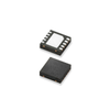
The LS0502SCD33 is a complete solution for system with backup storage capacitor or capacitor bank. It integrated input overvoltage, overcurrent protection circuit, a reverse blocking switch and super capacitor charging control circuit. It also has built-in cell balance to provide protection over two cell super capacitor system. When the main supply is present and above the minimum system supply voltage, system will draw power from input supply. At the same time, integrated linear charger charges the storage element at up to 300 mA current. Once the storage element is charged, the circuit draws only 2.5 μA of current while it maintains the super capacitor or other storage element in its ready state. When the main supply is removed, the integrated reverse blocking switch will block current flow from system rail to input. The linear charger will be turned on to provide power to system rail with low resistance path with up to 2 A current. Integrated cell balancing circuit will keep monitoring the cell voltage when charging and keep the two cells voltage at same level. The LS0502SCD33 is externally programmable for input current limit, input overvoltage, charge current limit, and charge voltage limit. It provides a flag signal when input supply is unplugged so that main system can taking action. LS0502SCD33 is available in DFN3X3-10 package.DFN Package 3.3 V to 5.5 V System Voltage 18 V Input Rating withOvervoltage Protection Programmable 1.1 V to 5.3 VCap Voltage Range Programmable SuperCapacitor Charge Current Programmable InputOvercurrent Protection Automatic Cell Balancing Automatic Main/BackupSwitchove r Up to 2 A Discharge Current Programmable Voltage and Current Thresholds ±2 % Threshold Accuracy
Datasheet
Description
The LS0502SCD33 is a complete solution for system with backup storage capacitor or capacitor bank. It integrated input overvoltage, overcurrent protection circuit, a reverse blocking switch and super capacitor charging control circuit. It also has built-in cell balance to provide protection over two cell super capacitor system. When the main supply is present and above the minimum system supply voltage, system will draw power from input supply. At the same time, integrated linear charger charges the storage element at up to 300 mA current. Once the storage element is charged, the circuit draws only 2.5 μA of current while it maintains the super capacitor or other storage element in its ready state. When the main supply is removed, the integrated reverse blocking switch will block current flow from system rail to input. The linear charger will be turned on to provide power to system rail with low resistance path with up to 2 A current. Integrated cell balancing circuit will keep monitoring the cell voltage when charging and keep the two cells voltage at same level. The LS0502SCD33 is externally programmable for input current limit, input overvoltage, charge current limit, and charge voltage limit. It provides a flag signal when input supply is unplugged so that main system can taking action. LS0502SCD33 is available in DFN3X3-10 package.DFN Package 3.3 V to 5.5 V System Voltage 18 V Input Rating withOvervoltage Protection Programmable 1.1 V to 5.3 VCap Voltage Range Programmable SuperCapacitor Charge Current Programmable InputOvercurrent Protection Automatic Cell Balancing Automatic Main/BackupSwitchove r Up to 2 A Discharge Current Programmable Voltage and Current Thresholds ±2 % Threshold Accuracy
Datasheet

Suppliers

Company
Product
Description
Supplier Links
Super Capacitor Protection IC for Backup Power Applications - LS0502SCD33 - Littelfuse, Inc.
Rosemont, IL, United States
Super Capacitor Protection IC for Backup Power Applications
LS0502SCD33
Super Capacitor Protection IC for Backup Power Applications LS0502SCD33
The LS0502SCD33 is a complete solution for system with backup storage capacitor or capacitor bank. It integrated input overvoltage, overcurrent protection circuit, a reverse blocking switch and super capacitor charging control circuit. It also has built-in cell balance to provide protection over two cell super capacitor system. When the main supply is present and above the minimum system supply voltage, system will draw power from input supply. At the same time, integrated linear charger charges the storage element at up to 300 mA current. Once the storage element is charged, the circuit draws only 2.5 μA of current while it maintains the super capacitor or other storage element in its ready state. When the main supply is removed, the integrated reverse blocking switch will block current flow from system rail to input. The linear charger will be turned on to provide power to system rail with low resistance path with up to 2 A current. Integrated cell balancing circuit will keep monitoring the cell voltage when charging and keep the two cells voltage at same level. The LS0502SCD33 is externally programmable for input current limit, input overvoltage, charge current limit, and charge voltage limit. It provides a flag signal when input supply is unplugged so that main system can taking action. LS0502SCD33 is available in DFN3X3-10 package.DFN Package 3.3 V to 5.5 V System Voltage 18 V Input Rating withOvervoltage Protection Programmable 1.1 V to 5.3 VCap Voltage Range Programmable SuperCapacitor Charge Current Programmable InputOvercurrent Protection Automatic Cell Balancing Automatic Main/BackupSwitchove r Up to 2 A Discharge Current Programmable Voltage and Current Thresholds ±2 % Threshold Accuracy

The LS0502SCD33 is a complete solution for system with backup storage capacitor or capacitor bank. It integrated input overvoltage, overcurrent protection circuit, a reverse blocking switch and super capacitor charging control circuit. It also has built-in cell balance to provide protection over two cell super capacitor system. When the main supply is present and above the minimum system supply voltage, system will draw power from input supply. At the same time, integrated linear charger charges the storage element at up to 300 mA current. Once the storage element is charged, the circuit draws only 2.5 μA of current while it maintains the super capacitor or other storage element in its ready state. When the main supply is removed, the integrated reverse blocking switch will block current flow from system rail to input. The linear charger will be turned on to provide power to system rail with low resistance path with up to 2 A current. Integrated cell balancing circuit will keep monitoring the cell voltage when charging and keep the two cells voltage at same level. The LS0502SCD33 is externally programmable for input current limit, input overvoltage, charge current limit, and charge voltage limit. It provides a flag signal when input supply is unplugged so that main system can taking action. LS0502SCD33 is available in DFN3X3-10 package.DFN Package 3.3 V to 5.5 V System Voltage 18 V Input Rating withOvervoltage Protection Programmable 1.1 V to 5.3 VCap Voltage Range Programmable SuperCapacitor Charge Current Programmable InputOvercurrent Protection Automatic Cell Balancing Automatic Main/BackupSwitchover Up to 2 A Discharge Current Programmable Voltage and Current Thresholds ±2 % Threshold Accuracy

Datasheet

Technical Specifications

  Littelfuse, Inc.
Product Category Fuses
Product Number LS0502SCD33
Product Name Super Capacitor Protection IC for Backup Power Applications
Unlock Full Specs
to access all available technical data

Similar Products

Power supply module for electronic circuit breaker - DF2101 - ifm efector inc.
Specs
Mounting Mounting on DIN rail; (TH35 (EN 60715))
Operating Temperature -25 to 60 C (-13 to 140 F)
Rated Voltage 30 volts
View Details
Specs
Mounting Panel Mount
Approvals / Standards RoHS
View Details
1494U 100A Fuse Block - 1494U-F100 - Allen-Bradley / Rockwell Automation
Allen-Bradley / Rockwell Automation
View Details
International Fuse Quick Acting 32mA - 81411101 - Interpower
Specs
Fuse Material Glass; Glass
Operating Temperature -25 to 70 C (-13 to 158 F)
Rated Voltage 250 volts
View Details