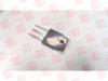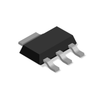
Littelfuse, Inc. FET for LITELINK™ phone line interface IC CPC5603

Description
Our N-channel depletion mode field effect transistors (FET) utilize a proprietary third generation vertical DMOS process. The third generation process realizes world-class, high voltage MOSFET performance in an economical silicon gate process. The vertical DMOS process yields a robust device for high power applications with high input impedance. These highly reliable FET devices have been used extensively in our solid state relays for industrial and telecommunications applications. Device Normally On High Breakdown Voltage Low On-Resistance Low VGS (off) Voltage Low On-Resistance at Cold Temperatures High Input Impedance Low Input and Output Leakage Small Package Size: SOT-23, SOT-89 & SOT-223
Datasheet
Description
Our N-channel depletion mode field effect transistors (FET) utilize a proprietary third generation vertical DMOS process. The third generation process realizes world-class, high voltage MOSFET performance in an economical silicon gate process. The vertical DMOS process yields a robust device for high power applications with high input impedance. These highly reliable FET devices have been used extensively in our solid state relays for industrial and telecommunications applications. Device Normally On High Breakdown Voltage Low On-Resistance Low VGS (off) Voltage Low On-Resistance at Cold Temperatures High Input Impedance Low Input and Output Leakage Small Package Size: SOT-23, SOT-89 & SOT-223
Datasheet

Suppliers

Company
Product
Description
Supplier Links
FET for LITELINK™ phone line interface IC - CPC5603 - Littelfuse, Inc.
Rosemont, IL, United States
FET for LITELINK™ phone line interface IC
CPC5603
FET for LITELINK™ phone line interface IC CPC5603
Our N-channel depletion mode field effect transistors (FET) utilize a proprietary third generation vertical DMOS process. The third generation process realizes world-class, high voltage MOSFET performance in an economical silicon gate process. The vertical DMOS process yields a robust device for high power applications with high input impedance. These highly reliable FET devices have been used extensively in our solid state relays for industrial and telecommunications applications. Device Normally On High Breakdown Voltage Low On-Resistance Low VGS (off) Voltage Low On-Resistance at Cold Temperatures High Input Impedance Low Input and Output Leakage Small Package Size: SOT-23, SOT-89 & SOT-223

Our N-channel depletion mode field effect transistors (FET) utilize a proprietary third generation vertical DMOS process. The third generation process realizes world-class, high voltage MOSFET performance in an economical silicon gate process. The vertical DMOS process yields a robust device for high power applications with high input impedance. These highly reliable FET devices have been used extensively in our solid state relays for industrial and telecommunications applications. Device Normally On High Breakdown Voltage Low On-Resistance Low VGS (off) Voltage Low On-Resistance at Cold Temperatures High Input Impedance Low Input and Output Leakage Small Package Size: SOT-23, SOT-89 & SOT-223

Supplier's Site Datasheet

Technical Specifications

  Littelfuse, Inc.
Product Category Transistors
Product Number CPC5603
Product Name FET for LITELINK™ phone line interface IC
Unlock Full Specs
to access all available technical data

Similar Products

TRANSISTORS - Transistors (BJT) - Single - 2SA1352E - 855029-2SA1352E - Win Source Electronics
Specs
Transistor Type Bipolar RF
Package Type SOT3
View Details
45 V, 500 mA NPN general-purpose transistors - BC817-40-QVL - Nexperia B.V.
Specs
Transistor Type BJT
Package Type SOT23; SOT23 SOT23
View Details
3 suppliers
DC - 3.6 GHz, 90 Watt, 48 Volt GaN RF Power Transistor - QPD0060 - Qorvo
Specs
Transistor Technology / Material DC - 3.6 GHz, 90 Watt, 48 Volt GaN RF Power Transistor
Package Type DFN
View Details