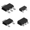
Littelfuse, Inc. N-channel depletion mode field effect transistors (FET) CPC3902

Description
Our N-channel depletion mode field effect transistors (FET) utilize a proprietary third generation vertical DMOS process. The third generation process realizes world-class, high voltage MOSFET performance in an economical silicon gate process. The vertical DMOS process yields a robust device for high power applications with high input impedance. These highly reliable FET devices have been used extensively in our solid state relays for industrial and telecommunications applications. Device Normally On High Breakdown Voltage Low On-Resistance Low VGS (off) Voltage Low On-Resistance at Cold Temperatures High Input Impedance Low Input and Output Leakage Small Package Size: SOT-23, SOT-89 & SOT-223
Datasheet
Datasheet Summary
Powered by GS/AI

The CPC3902 is a 250V, N-channel, depletion-mode MOSFET in an SOT-223 package, designed for high-power applications such as current regulation, normally-on switching, and solid state relays. It has a maximum on-resistance of 2.5Ω at 25°C and a gate-to-source off voltage range of -1.4V to -3.1V. The device supports a continuous drain current of 400mA and a total package dissipation of 1.8W when mounted on a 1"×1" 2 oz. copper FR4 board. Thermal resistance is 14°C/W from junction to case and 55°C/W from junction to ambient. It operates from -55°C to +110°C with a maximum junction temperature of +125°C. The part meets MSL 1 moisture sensitivity and ESD sensitivity per JESD-625, with a reflow soldering profile of 260°C for 30 seconds. Input capacitance is 230pF at VGS = -3.5V, and reverse transfer capacitance is 9.5pF at 1MHz.

Suppliers

Company
Product
Description
Supplier Links
N-channel depletion mode field effect transistors (FET) - CPC3902 - Littelfuse, Inc.
Rosemont, IL, United States
N-channel depletion mode field effect transistors (FET)
CPC3902
N-channel depletion mode field effect transistors (FET) CPC3902
Our N-channel depletion mode field effect transistors (FET) utilize a proprietary third generation vertical DMOS process. The third generation process realizes world-class, high voltage MOSFET performance in an economical silicon gate process. The vertical DMOS process yields a robust device for high power applications with high input impedance. These highly reliable FET devices have been used extensively in our solid state relays for industrial and telecommunications applications. Device Normally On High Breakdown Voltage Low On-Resistance Low VGS (off) Voltage Low On-Resistance at Cold Temperatures High Input Impedance Low Input and Output Leakage Small Package Size: SOT-23, SOT-89 & SOT-223

Our N-channel depletion mode field effect transistors (FET) utilize a proprietary third generation vertical DMOS process. The third generation process realizes world-class, high voltage MOSFET performance in an economical silicon gate process. The vertical DMOS process yields a robust device for high power applications with high input impedance. These highly reliable FET devices have been used extensively in our solid state relays for industrial and telecommunications applications. Device Normally On High Breakdown Voltage Low On-Resistance Low VGS (off) Voltage Low On-Resistance at Cold Temperatures High Input Impedance Low Input and Output Leakage Small Package Size: SOT-23, SOT-89 & SOT-223

Supplier's Site Datasheet

Technical Specifications

  Littelfuse, Inc.
Product Category Transistors
Product Number CPC3902
Product Name N-channel depletion mode field effect transistors (FET)
Polarity N-Channel
Unlock Full Specs
to access all available technical data

Similar Products

7 Watt, 50 Volt, 0.03 - 1.2 GHz, GaN RF Input-Matched Transistor - QPD1011 - Qorvo
Specs
Transistor Technology / Material GaN
Package Type DFN / SMT
View Details
TRANSISTORS - Transistors (BJT) - Single - 2SA1006B-AZ - 906299-2SA1006B-AZ - Win Source Electronics
Specs
Transistor Type Bipolar RF
Package Type SOT3
View Details
 - LM5051MA/NOPB - Rochester Electronics
Texas Instruments
Specs
Transistor Type MOSFET
Package Type SOIC8
View Details
650V 6.2A TO-252 MOSFET Transistor - 285-06N60C3 - ERSAELECTRONICS PTE. LTD.
Specs
Transistor Type MOSFET
Polarity N-Channel
Package Type Reel - TR
View Details
2 suppliers