Integrated Device Technology 6-output Differential Buffer For PCIe Gen2 9DB106BFLFT

Description
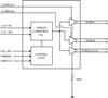
The 9DB106 zero-delay buffer supports PCIe Gen1 and Gen2 clocking requirements. The 9DB106 is driven by a differential SRC output pair from an IDT CK410 / CK505 -compliant main clock generator. It attenuates jitter on the input clock and has a selectable PLL bandwidth to maximize performance in systems with or without Spread-Spectrum clocking. An SMBus interface allows control of the PLL bandwidth and bypass options, while 2 clock request ( CLKREQ #) pins make the 9DB106 suitable for Express Card applications.
Datasheet
Description
The 9DB106 zero-delay buffer supports PCIe Gen1 and Gen2 clocking requirements. The 9DB106 is driven by a differential SRC output pair from an IDT CK410 / CK505 -compliant main clock generator. It attenuates jitter on the input clock and has a selectable PLL bandwidth to maximize performance in systems with or without Spread-Spectrum clocking. An SMBus interface allows control of the PLL bandwidth and bypass options, while 2 clock request ( CLKREQ #) pins make the 9DB106 suitable for Express Card applications.
Datasheet

Suppliers

Company
Product
Description
Supplier Links
6-output Differential Buffer For PCIe Gen2 - 9DB106BFLFT - Integrated Device Technology
San Jose, CA, USA
6-output Differential Buffer For PCIe Gen2
9DB106BFLFT
6-output Differential Buffer For PCIe Gen2 9DB106BFLFT
The 9DB106 zero-delay buffer supports PCIe Gen1 and Gen2 clocking requirements. The 9DB106 is driven by a differential SRC output pair from an IDT CK410 / CK505 -compliant main clock generator. It attenuates jitter on the input clock and has a selectable PLL bandwidth to maximize performance in systems with or without Spread-Spectrum clocking. An SMBus interface allows control of the PLL bandwidth and bypass options, while 2 clock request ( CLKREQ #) pins make the 9DB106 suitable for Express Card applications.

The 9DB106 zero-delay buffer supports PCIe Gen1 and Gen2 clocking requirements. The 9DB106 is driven by a differential SRC output pair from an IDT CK410 / CK505 -compliant main clock generator. It attenuates jitter on the input clock and has a selectable PLL bandwidth to maximize performance in systems with or without Spread-Spectrum clocking. An SMBus interface allows control of the PLL bandwidth and bypass options, while 2 clock request ( CLKREQ #) pins make the 9DB106 suitable for Express Card applications.

Supplier's Site Datasheet

Technical Specifications

  Integrated Device Technology
Product Category IC Interfaces
Product Number 9DB106BFLFT
Product Name 6-output Differential Buffer For PCIe Gen2
Technology PCI Express
Device Type Buffer
Supply Voltage 3.3V
Pd 429 milliwatts
Unlock Full Specs
to access all available technical data

Similar Products

Sensor and Detector Interfaces - A5367CA-T-ND - DigiKey
Specs
Device Type Sensor Interface
Operating Temperature -10 to 60 C (14 to 140 F)
Package Type DIP; "16-DIP (0.300"", 7.62mm)"
View Details
4 suppliers
RF Front End (LNA + PA) - 2312-QPF4588TR13-5KTR-ND - DigiKey
Specs
Device Type Front End
Package Type 24-VFQFN Exposed Pad
Pins 24 #
View Details
Interface module - 289-619 - WAGO
Specs
Device Type Sensor Interface
Operating Temperature -20 to 55 C (-4 to 131 F)
View Details
Telecom - SI3225-G-FQR - Quarktwin Technology Ltd.
Skyworks Solutions, Inc.
Specs
Technology SPI; GCI, PCM, SPI
Features RoHS
Supply Voltage 5V; Other; 3.3V, 5V
View Details