Integrated Device Technology Differential-to-LVCMOS/LVTTL Fanout Buffer W/Divider And Glitchless Switch 870S208BKLF

Description
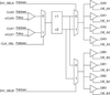
The 870S208 is a low skew, 8 output LVCMOS / LVTTL Fanout Buffer with selectable divider. The 870S208 has 2 selectable inputs that accept a variety of differential input types. The device provides the capability to suppress any glitch at the outputs of the device during an input clock switch to enhance clock redundancy in fault tolerant applications. The low impedance LVCMOS outputs are designed to drive 50? series or parallel terminated transmission lines. The effective fanout can be increased from 8 to 16 by utilizing the ability of the outputs to drive two series terminated lines. The divide select inputs, DIV_SELA and DIV_SELB, control the output frequency of each bank. The output banks can be independently selected for ÷1 or ÷2 operation. The output enable pins assigned to each output, support enabling and disabling of each output individually. The 870S208 is characterized at full 3.3V and 2.5V, and mixed 3.3V/2.5V output operating supply modes. Guaranteed output and part-to-part skew characteristics make the 870S208 ideal for high performance, single ended applications.
Datasheet
Description
The 870S208 is a low skew, 8 output LVCMOS / LVTTL Fanout Buffer with selectable divider. The 870S208 has 2 selectable inputs that accept a variety of differential input types. The device provides the capability to suppress any glitch at the outputs of the device during an input clock switch to enhance clock redundancy in fault tolerant applications. The low impedance LVCMOS outputs are designed to drive 50? series or parallel terminated transmission lines. The effective fanout can be increased from 8 to 16 by utilizing the ability of the outputs to drive two series terminated lines. The divide select inputs, DIV_SELA and DIV_SELB, control the output frequency of each bank. The output banks can be independently selected for ÷1 or ÷2 operation. The output enable pins assigned to each output, support enabling and disabling of each output individually. The 870S208 is characterized at full 3.3V and 2.5V, and mixed 3.3V/2.5V output operating supply modes. Guaranteed output and part-to-part skew characteristics make the 870S208 ideal for high performance, single ended applications.
Datasheet

Suppliers

Company
Product
Description
Supplier Links
Differential-to-LVCMOS/LVTTL Fanout Buffer W/Divider And Glitchless Switch - 870S208BKLF - Integrated Device Technology
San Jose, CA, USA
Differential-to-LVCMOS/LVTTL Fanout Buffer W/Divider And Glitchless Switch
870S208BKLF
Differential-to-LVCMOS/LVTTL Fanout Buffer W/Divider And Glitchless Switch 870S208BKLF
The 870S208 is a low skew, 8 output LVCMOS / LVTTL Fanout Buffer with selectable divider. The 870S208 has 2 selectable inputs that accept a variety of differential input types. The device provides the capability to suppress any glitch at the outputs of the device during an input clock switch to enhance clock redundancy in fault tolerant applications. The low impedance LVCMOS outputs are designed to drive 50? series or parallel terminated transmission lines. The effective fanout can be increased from 8 to 16 by utilizing the ability of the outputs to drive two series terminated lines. The divide select inputs, DIV_SELA and DIV_SELB, control the output frequency of each bank. The output banks can be independently selected for ÷1 or ÷2 operation. The output enable pins assigned to each output, support enabling and disabling of each output individually. The 870S208 is characterized at full 3.3V and 2.5V, and mixed 3.3V/2.5V output operating supply modes. Guaranteed output and part-to-part skew characteristics make the 870S208 ideal for high performance, single ended applications.

The 870S208 is a low skew, 8 output LVCMOS / LVTTL Fanout Buffer with selectable divider. The 870S208 has 2 selectable inputs that accept a variety of differential input types. The device provides the capability to suppress any glitch at the outputs of the device during an input clock switch to enhance clock redundancy in fault tolerant applications. The low impedance LVCMOS outputs are designed to drive 50? series or parallel terminated transmission lines. The effective fanout can be increased from 8 to 16 by utilizing the ability of the outputs to drive two series terminated lines. The divide select inputs, DIV_SELA and DIV_SELB, control the output frequency of each bank. The output banks can be independently selected for ÷1 or ÷2 operation. The output enable pins assigned to each output, support enabling and disabling of each output individually. The 870S208 is characterized at full 3.3V and 2.5V, and mixed 3.3V/2.5V output operating supply modes. Guaranteed output and part-to-part skew characteristics make the 870S208 ideal for high performance, single ended applications.

Supplier's Site Datasheet

Technical Specifications

  Integrated Device Technology
Product Category IC Interfaces
Product Number 870S208BKLF
Product Name Differential-to-LVCMOS/LVTTL Fanout Buffer W/Divider And Glitchless Switch
Technology CMOS
Device Type Buffer
Supply Voltage 2.5V; 3.3V
Unlock Full Specs
to access all available technical data

Similar Products

RF and mmW Front End Module - SE2442L-R - Richardson RFPD
Specs
Device Type Front End
Supply Voltage 3.6V; Other; 3.6
Package Type QFNL; QFN
View Details
Inverting Schmitt trigger - 74AHCT1G14GW,118 - Nexperia B.V.
Specs
Technology TTL
Supply Voltage 5V; Other; 4.5 - 5.5
Operating Temperature -40 to 125 C (-40 to 257 F)
View Details
Line Interface ICs - 1460474 - RS Components, Ltd.
Specs
Device Type Line / Bus Driver; Buffer; Buffer, driver
Features RoHS
Supply Voltage Other; 5.5 v
View Details
SN54BCT543 Octal Registered Transceivers With 3-State Outputs - 5962-9087001M3A - Texas Instruments
Specs
Technology BCT
Device Type Transceiver
Supply Voltage Other; 5.5
View Details