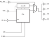

The 86004I is a high performance 1:4 LVCMOS / LVTTL Clock Buffer. The 86004I has a fully integrated PLL and can be configured as zero delay buffer and has an input and output frequency range of 15.625MHz to 62.5MHz. The VCO operates at a frequency range of 250MHz to 500MHz. The external feedback allows the device to achieve "zero delay" between the input clock and the output clocks. The PLL_SEL pin can be used to bypass the PLL for system test and debug purposes. In bypass mode, the reference clock is routed around the PLL and into the internal output divider.
| Integrated Device Technology | |
|---|---|
| Product Category | IC Interfaces |
| Product Number | 86004BGILFT |
| Product Name | 15.625MHz to 62.5MHz, 1:4 LVCMOS/LVTTL Zero Delay Clock Buffer |
| Technology | CMOS |
| Device Type | Buffer |
| Supply Voltage | 2.5V; 3.3V |