Integrated Device Technology Dual Output RF Frequency Synthesizer 844S42BKILFT

Description
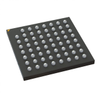
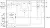
The 844S42I is a 3.3V compatible, PLL based clock synthesizer targeted for clock generation in high-performance instrumentation, networking and computing applications. Using either the serial ( I2C ) or parallel programming interface, the 844S42I enables the generation of clock frequencies in the range of 81MHz to 2592MHz. The internal crystal oscillator uses the external quartz crystal as the basis of its frequency reference. Alternatively, a LVCMOS compatible clock signal can be used as PLL reference signal. The devices uses an integer-N synthesizer architecture and is optimized for low-jitter generation. The VCO within the PLL operates over a range of 1296MHz to 2592MHz. Its output is scaled by a divider that is configured by either the I2C or parallel interfaces. The crystal oscillator frequency fXTAL, the PLL pre-divider P, the feedback-divider M and the PLL post-divider N determine the output frequency. The feedback path of the PLL is internal. The PLL post-dividers NA and NB are configured through either the I2C or the parallel interfaces, each can provide one of seven division ratios (1, 2, 3, 4, 6, 8, 16). This divider extends the performance of the part while providing a typical 50% duty cycle. The high-frequency outputs QA and QB are differential and are capable of driving a pair of transmission lines. The positive supply voltage for the internal PLL is separated from the power supply for the core logic and output drivers to minimize noise induced jitter. The serial interface is I2C compatible and provides read and write access to the internal PLL configuration registers. The lock state of the PLL is indicated by the LVCMOS -compatible LOCK_DT output. This device provides a clock enable control input that, when active ( LOW ), allows the outputs to switch normally, and when inactive ( HIGH ), places the outputs in a high impedance state. The 844S42I is packaged in a 8mm x 8mm 56-lead VFQFN package.
Datasheet
Description
The 844S42I is a 3.3V compatible, PLL based clock synthesizer targeted for clock generation in high-performance instrumentation, networking and computing applications. Using either the serial ( I2C ) or parallel programming interface, the 844S42I enables the generation of clock frequencies in the range of 81MHz to 2592MHz. The internal crystal oscillator uses the external quartz crystal as the basis of its frequency reference. Alternatively, a LVCMOS compatible clock signal can be used as PLL reference signal. The devices uses an integer-N synthesizer architecture and is optimized for low-jitter generation. The VCO within the PLL operates over a range of 1296MHz to 2592MHz. Its output is scaled by a divider that is configured by either the I2C or parallel interfaces. The crystal oscillator frequency fXTAL, the PLL pre-divider P, the feedback-divider M and the PLL post-divider N determine the output frequency. The feedback path of the PLL is internal. The PLL post-dividers NA and NB are configured through either the I2C or the parallel interfaces, each can provide one of seven division ratios (1, 2, 3, 4, 6, 8, 16). This divider extends the performance of the part while providing a typical 50% duty cycle. The high-frequency outputs QA and QB are differential and are capable of driving a pair of transmission lines. The positive supply voltage for the internal PLL is separated from the power supply for the core logic and output drivers to minimize noise induced jitter. The serial interface is I2C compatible and provides read and write access to the internal PLL configuration registers. The lock state of the PLL is indicated by the LVCMOS -compatible LOCK_DT output. This device provides a clock enable control input that, when active ( LOW ), allows the outputs to switch normally, and when inactive ( HIGH ), places the outputs in a high impedance state. The 844S42I is packaged in a 8mm x 8mm 56-lead VFQFN package.
Datasheet

Suppliers

Company
Product
Description
Supplier Links
Dual Output RF Frequency Synthesizer - 844S42BKILFT - Integrated Device Technology
San Jose, CA, USA
Dual Output RF Frequency Synthesizer
844S42BKILFT
Dual Output RF Frequency Synthesizer 844S42BKILFT
The 844S42I is a 3.3V compatible, PLL based clock synthesizer targeted for clock generation in high-performance instrumentation, networking and computing applications. Using either the serial ( I2C ) or parallel programming interface, the 844S42I enables the generation of clock frequencies in the range of 81MHz to 2592MHz. The internal crystal oscillator uses the external quartz crystal as the basis of its frequency reference. Alternatively, a LVCMOS compatible clock signal can be used as PLL reference signal. The devices uses an integer-N synthesizer architecture and is optimized for low-jitter generation. The VCO within the PLL operates over a range of 1296MHz to 2592MHz. Its output is scaled by a divider that is configured by either the I2C or parallel interfaces. The crystal oscillator frequency fXTAL, the PLL pre-divider P, the feedback-divider M and the PLL post-divider N determine the output frequency. The feedback path of the PLL is internal. The PLL post-dividers NA and NB are configured through either the I2C or the parallel interfaces, each can provide one of seven division ratios (1, 2, 3, 4, 6, 8, 16). This divider extends the performance of the part while providing a typical 50% duty cycle. The high-frequency outputs QA and QB are differential and are capable of driving a pair of transmission lines. The positive supply voltage for the internal PLL is separated from the power supply for the core logic and output drivers to minimize noise induced jitter. The serial interface is I2C compatible and provides read and write access to the internal PLL configuration registers. The lock state of the PLL is indicated by the LVCMOS -compatible LOCK_DT output. This device provides a clock enable control input that, when active ( LOW ), allows the outputs to switch normally, and when inactive ( HIGH ), places the outputs in a high impedance state. The 844S42I is packaged in a 8mm x 8mm 56-lead VFQFN package.

The 844S42I is a 3.3V compatible, PLL based clock synthesizer targeted for clock generation in high-performance instrumentation, networking and computing applications. Using either the serial ( I2C ) or parallel programming interface, the 844S42I enables the generation of clock frequencies in the range of 81MHz to 2592MHz. The internal crystal oscillator uses the external quartz crystal as the basis of its frequency reference. Alternatively, a LVCMOS compatible clock signal can be used as PLL reference signal. The devices uses an integer-N synthesizer architecture and is optimized for low-jitter generation. The VCO within the PLL operates over a range of 1296MHz to 2592MHz. Its output is scaled by a divider that is configured by either the I2C or parallel interfaces. The crystal oscillator frequency fXTAL, the PLL pre-divider P, the feedback-divider M and the PLL post-divider N determine the output frequency. The feedback path of the PLL is internal. The PLL post-dividers NA and NB are configured through either the I2C or the parallel interfaces, each can provide one of seven division ratios (1, 2, 3, 4, 6, 8, 16). This divider extends the performance of the part while providing a typical 50% duty cycle. The high-frequency outputs QA and QB are differential and are capable of driving a pair of transmission lines. The positive supply voltage for the internal PLL is separated from the power supply for the core logic and output drivers to minimize noise induced jitter. The serial interface is I2C compatible and provides read and write access to the internal PLL configuration registers. The lock state of the PLL is indicated by the LVCMOS -compatible LOCK_DT output. This device provides a clock enable control input that, when active ( LOW ), allows the outputs to switch normally, and when inactive ( HIGH ), places the outputs in a high impedance state. The 844S42I is packaged in a 8mm x 8mm 56-lead VFQFN package.

Supplier's Site Datasheet

Technical Specifications

  Integrated Device Technology
Product Category IC Phase-locked Loops (PLL)
Product Number 844S42BKILFT
Product Name Dual Output RF Frequency Synthesizer
Bus Interface LVPECL; LVDS; LVPECL,LVDS
Package Type Surface Mount; VFQFPN
Supply Voltage 3.3 volts
Unlock Full Specs
to access all available technical data

Similar Products

CD4046B CMOS Micropower Phase-Locked Loop - CD4046BNSR - Texas Instruments
Specs
Bus Interface CMOS
Package Type PDIP,SO,TSSOP
Supply Voltage 3 to 18 volts
View Details
9 suppliers
Clock and Timing IC - 763-SI52112-B3-GTR - ERSAELECTRONICS PTE. LTD.
Specs
Bus Interface HCSL
Package Type Tape & Reel (TR)
Supply Voltage 2.97 to 3.63 volts
View Details
3 suppliers
Clock Generators, PLLs, Frequency Synthesizers - 1727-3465-ND - DigiKey
Specs
Bus Interface Clock
Package Type Surface Mount; TSSOP; "16-TSSOP (0.173"", 4.40mm Width)"
Supply Voltage 4.5 to 5.5 volts
View Details
4 suppliers