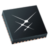
Integrated Device Technology VCXO Jitter Attenuator & Femtoclock NG Multiplier 813N252BKI-04LFT

Description
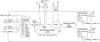
The 813N252I -04 is a PLL based synchronous multiplier that is optimized for PDH or SONET to Ethernet clock jitter attenuation and frequency translation. The device contains two internal frequency multiplication stages that are cascaded in series. The first stage is a VCXO PLL that is optimized to provide reference clock jitter attenuation. The second stage is a FemtoClock® NG frequency multiplier that provides the low jitter, high frequency Ethernet output clock that easily meets Gigabit and 10 Gigabit Ethernet jitter requirements. Pre-divider and output divider multiplication ratios are selected using device selection control pins. The multiplication ratios are optimized to support most common clock rates used in PDH , SONET and Ethernet applications. The VCXO requires the use of an external, inexpensive pullable crystal. The VCXO uses external passive loop filter components which allows configuration of the PLL loop bandwidth and damping characteristics. The device is packaged in a space-saving 32- VFQFN package and supports industrial temperature range.
Datasheet
Description
The 813N252I -04 is a PLL based synchronous multiplier that is optimized for PDH or SONET to Ethernet clock jitter attenuation and frequency translation. The device contains two internal frequency multiplication stages that are cascaded in series. The first stage is a VCXO PLL that is optimized to provide reference clock jitter attenuation. The second stage is a FemtoClock® NG frequency multiplier that provides the low jitter, high frequency Ethernet output clock that easily meets Gigabit and 10 Gigabit Ethernet jitter requirements. Pre-divider and output divider multiplication ratios are selected using device selection control pins. The multiplication ratios are optimized to support most common clock rates used in PDH , SONET and Ethernet applications. The VCXO requires the use of an external, inexpensive pullable crystal. The VCXO uses external passive loop filter components which allows configuration of the PLL loop bandwidth and damping characteristics. The device is packaged in a space-saving 32- VFQFN package and supports industrial temperature range.
Datasheet

Suppliers

Company
Product
Description
Supplier Links
VCXO Jitter Attenuator & Femtoclock NG Multiplier - 813N252BKI-04LFT - Integrated Device Technology
San Jose, CA, USA
VCXO Jitter Attenuator & Femtoclock NG Multiplier
813N252BKI-04LFT
VCXO Jitter Attenuator & Femtoclock NG Multiplier 813N252BKI-04LFT
The 813N252I -04 is a PLL based synchronous multiplier that is optimized for PDH or SONET to Ethernet clock jitter attenuation and frequency translation. The device contains two internal frequency multiplication stages that are cascaded in series. The first stage is a VCXO PLL that is optimized to provide reference clock jitter attenuation. The second stage is a FemtoClock® NG frequency multiplier that provides the low jitter, high frequency Ethernet output clock that easily meets Gigabit and 10 Gigabit Ethernet jitter requirements. Pre-divider and output divider multiplication ratios are selected using device selection control pins. The multiplication ratios are optimized to support most common clock rates used in PDH , SONET and Ethernet applications. The VCXO requires the use of an external, inexpensive pullable crystal. The VCXO uses external passive loop filter components which allows configuration of the PLL loop bandwidth and damping characteristics. The device is packaged in a space-saving 32- VFQFN package and supports industrial temperature range.

The 813N252I -04 is a PLL based synchronous multiplier that is optimized for PDH or SONET to Ethernet clock jitter attenuation and frequency translation. The device contains two internal frequency multiplication stages that are cascaded in series. The first stage is a VCXO PLL that is optimized to provide reference clock jitter attenuation. The second stage is a FemtoClock® NG frequency multiplier that provides the low jitter, high frequency Ethernet output clock that easily meets Gigabit and 10 Gigabit Ethernet jitter requirements. Pre-divider and output divider multiplication ratios are selected using device selection control pins. The multiplication ratios are optimized to support most common clock rates used in PDH , SONET and Ethernet applications. The VCXO requires the use of an external, inexpensive pullable crystal. The VCXO uses external passive loop filter components which allows configuration of the PLL loop bandwidth and damping characteristics. The device is packaged in a space-saving 32- VFQFN package and supports industrial temperature range.

Supplier's Site Datasheet

Technical Specifications

  Integrated Device Technology
Product Category IC Phase-locked Loops (PLL)
Product Number 813N252BKI-04LFT
Product Name VCXO Jitter Attenuator & Femtoclock NG Multiplier
Bus Interface LVPECL; LVDS; LVPECL,LVDS
Package Type Surface Mount; VFQFPN
Supply Voltage 3.3 volts
Unlock Full Specs
to access all available technical data

Similar Products

4046A Clock and Timing IC - 728-74HC4046ADB,112 - ERSAELECTRONICS PTE. LTD.
Specs
Operating Temperature -40 C (-40 F)
View Details
4 suppliers
Clock and Timing IC - 728-SI5326C-C-GMR - ERSAELECTRONICS PTE. LTD.
Skyworks Solutions, Inc.
Specs
Bus Interface CML, LVCMOS, LVDS, LVPECL
Package Type Tape & Reel (TR)
Supply Voltage 1.71 to 3.63 volts
View Details
6 suppliers
Clock/Timing - Clock/Timing - Clock Generators, PLLs, Frequency Synthesizers - ADF4118YRUZ - 859973-ADF4118YRUZ - Win Source Electronics
Specs
Package Type Surface Mount; 16-TSSOP
Operating Temperature -40 to 125 C (-40 to 257 F)
View Details
2 suppliers
CDCEL913 Programmable 1-PLL VCXO Clock Synthesizer with 1.8-V LVCMOS Outputs - CDCEL913PWG4 - Texas Instruments
Specs
Bus Interface LVCMOS
Package Type TSSOP
Supply Voltage 1.8 volts
View Details