Integrated Device Technology Clock Distribution Circuit 6T39007ANLGI8

Description
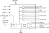
The IDT6T39007A is a low-power, four output clock distribution circuit. The device takes a TCXO or 1.8 V to 2.5 V LVCMOS input and generates four high-quality LVDS outputs, and two programmable divided outputs. It includes a redundant input with automatic glitch-free switching when the primary reference is removed. The primary input may be selected by the user by pulling the SEL pin low or high. If the primary input is removed and brought back, it will not be re-selected until 1024 cycles have passed. The IDT6T39007A specifically addresses the needs of handheld applications in both performance and package size. The device is packaged in a small 4mm x 4mm 24-pin QFN , allowing optimal use for limited board space.
Datasheet
Description
The IDT6T39007A is a low-power, four output clock distribution circuit. The device takes a TCXO or 1.8 V to 2.5 V LVCMOS input and generates four high-quality LVDS outputs, and two programmable divided outputs. It includes a redundant input with automatic glitch-free switching when the primary reference is removed. The primary input may be selected by the user by pulling the SEL pin low or high. If the primary input is removed and brought back, it will not be re-selected until 1024 cycles have passed. The IDT6T39007A specifically addresses the needs of handheld applications in both performance and package size. The device is packaged in a small 4mm x 4mm 24-pin QFN , allowing optimal use for limited board space.
Datasheet

Suppliers

Company
Product
Description
Supplier Links
Clock Distribution Circuit - 6T39007ANLGI8 - Integrated Device Technology
San Jose, CA, USA
Clock Distribution Circuit
6T39007ANLGI8
Clock Distribution Circuit 6T39007ANLGI8
The IDT6T39007A is a low-power, four output clock distribution circuit. The device takes a TCXO or 1.8 V to 2.5 V LVCMOS input and generates four high-quality LVDS outputs, and two programmable divided outputs. It includes a redundant input with automatic glitch-free switching when the primary reference is removed. The primary input may be selected by the user by pulling the SEL pin low or high. If the primary input is removed and brought back, it will not be re-selected until 1024 cycles have passed. The IDT6T39007A specifically addresses the needs of handheld applications in both performance and package size. The device is packaged in a small 4mm x 4mm 24-pin QFN , allowing optimal use for limited board space.

The IDT6T39007A is a low-power, four output clock distribution circuit. The device takes a TCXO or 1.8 V to 2.5 V LVCMOS input and generates four high-quality LVDS outputs, and two programmable divided outputs. It includes a redundant input with automatic glitch-free switching when the primary reference is removed. The primary input may be selected by the user by pulling the SEL pin low or high. If the primary input is removed and brought back, it will not be re-selected until 1024 cycles have passed. The IDT6T39007A specifically addresses the needs of handheld applications in both performance and package size. The device is packaged in a small 4mm x 4mm 24-pin QFN , allowing optimal use for limited board space.

Supplier's Site Datasheet

Technical Specifications

  Integrated Device Technology
Product Category IC Interfaces
Product Number 6T39007ANLGI8
Product Name Clock Distribution Circuit
Device Type Buffer
Unlock Full Specs
to access all available technical data

Similar Products

RF Front End (LNA + PA) - 2312-QPB9329TR13TR-ND - DigiKey
Specs
Device Type Front End
Package Type 44-SMD Module
Pins 44 #
View Details
SN54HC366 Hex Bus Drivers With 3-State Outputs - 5962-8682801EA - Texas Instruments
Specs
Technology HC
Device Type Line / Bus Driver
Operating Temperature -55 to 125 C (-67 to 257 F)
View Details
Interface adapters - 857-980 - WAGO
Specs
Device Type Sensor Interface
Operating Temperature -25 to 70 C (-13 to 158 F)
View Details
Interface - Specialized - 5962-85016013A - Lingto Electronic Limited
Specs
Device Type Sensor Interface
View Details