Integrated Device Technology 2.5V to 3.3V High Performance Clock Buffer 5V2310PGG

Description
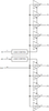
The IDT5V2310 is a high performance, low skew clock buffer that operates up to 200MHz. Two banks of five outputs each provide low skewcopies of CLK . Through the use of control pins 1G and 2G, the outputs of banks 1Y(0:4) and 2Y(0:4) can be placed in a low state regardless of CLKinput. The device operates in 2.5V and 3.3V environments. The built-in output enable glitch suppression ensures a synchronized output enablesequence to distribute full period clock signals. The IDT5V2310 is characterized for operation from -40°C to +85°C.
Datasheet
Description
The IDT5V2310 is a high performance, low skew clock buffer that operates up to 200MHz. Two banks of five outputs each provide low skewcopies of CLK . Through the use of control pins 1G and 2G, the outputs of banks 1Y(0:4) and 2Y(0:4) can be placed in a low state regardless of CLKinput. The device operates in 2.5V and 3.3V environments. The built-in output enable glitch suppression ensures a synchronized output enablesequence to distribute full period clock signals. The IDT5V2310 is characterized for operation from -40°C to +85°C.
Datasheet

Suppliers

Company
Product
Description
Supplier Links
2.5V to 3.3V High Performance Clock Buffer - 5V2310PGG - Integrated Device Technology
San Jose, CA, USA
2.5V to 3.3V High Performance Clock Buffer
5V2310PGG
2.5V to 3.3V High Performance Clock Buffer 5V2310PGG
The IDT5V2310 is a high performance, low skew clock buffer that operates up to 200MHz. Two banks of five outputs each provide low skewcopies of CLK . Through the use of control pins 1G and 2G, the outputs of banks 1Y(0:4) and 2Y(0:4) can be placed in a low state regardless of CLKinput. The device operates in 2.5V and 3.3V environments. The built-in output enable glitch suppression ensures a synchronized output enablesequence to distribute full period clock signals. The IDT5V2310 is characterized for operation from -40°C to +85°C.

The IDT5V2310 is a high performance, low skew clock buffer that operates up to 200MHz. Two banks of five outputs each provide low skewcopies of CLK . Through the use of control pins 1G and 2G, the outputs of banks 1Y(0:4) and 2Y(0:4) can be placed in a low state regardless of CLKinput. The device operates in 2.5V and 3.3V environments. The built-in output enable glitch suppression ensures a synchronized output enablesequence to distribute full period clock signals. The IDT5V2310 is characterized for operation from -40°C to +85°C.

Supplier's Site Datasheet

Technical Specifications

  Integrated Device Technology
Product Category IC Interfaces
Product Number 5V2310PGG
Product Name 2.5V to 3.3V High Performance Clock Buffer
Device Type Buffer
Unlock Full Specs
to access all available technical data

Similar Products

Interface Transceiver IC - 704-BTS7008-2EPA - ERSAELECTRONICS PTE. LTD.
Specs
Device Type Transceiver
Package Type Bulk
View Details
CY54FCT240T Octal Buffers/Drivers with 3-State Outputs - 5962-9221303MRA - Texas Instruments
Specs
Technology FCT
Device Type Buffer
Operating Temperature -55 to 125 C (-67 to 257 F)
View Details
3 suppliers
Hex inverting Schmitt trigger - 74AHCT14D-Q100,118 - Nexperia B.V.
Specs
Features RoHS
Supply Voltage Other; +7.0
Package Type SOT108-1 SOT108-1
View Details
 - A5947KLPTR-B-T - Rochester Electronics
Allegro MicroSystems Inc.
Specs
Features RoHS
Package Type SOP; SSOP; TSSOP; TSSOP-20
View Details