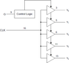

The IDT5V2305 is a high performance, low skew clock buffer that operates up to 200MHz. One bank of five outputs provides low skew copies of CLK . Through the use of control pin G, the outputs of bank Y(0:4) can be placed in a low state regardless of CLK input. The device operates in 2.5V and 3.3V environments. The built-in output enable glitch suppression ensures a synchronized output enable sequence to distribute full period clock signals. The IDT5V2305 is characterized for operation from -40°C to +85°C.
| Integrated Device Technology | |
|---|---|
| Product Category | IC Interfaces |
| Product Number | 5V2305NRGI8 |
| Product Name | 2.5V to 3.3V High Performance Clock Buffer |
| Device Type | Buffer |