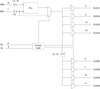

The IDT2308 is a high-speed phase-lock loop ( PLL ) clock multiplier. It is designed to address high-speed clock distribution and multiplication applications. The zero delay is achieved by aligning the phase between the incoming clock and the output clock, operable within the range of 10 to 133MHz. The IDT2308 has two banks of four outputs each that are controlled via two select addresses. By proper selection of input addresses, both banks can be put in tri-state mode. In test mode, the PLL is turned off, and the input clock directly drives the outputs for system testing purposes. In the absence of an input clock, the IDT2308 enters power down, and the outputs are tri-stated. In this mode, the device will draw less than 25μA. The IDT2308 is available in six unique configurations for both prescaling and multiplication of the Input REF Clock. (See available options table.) The PLL is closed externally to provide more flexibility by allowing the user to control the delay between the input clock and the outputs. The IDT2308 is characterized for both Industrial and Commercial operation.
| Integrated Device Technology | |
|---|---|
| Product Category | IC Interfaces |
| Product Number | 2308-2HPGG8 |
| Product Name | 3.3V Zero Delay Clock Multiplier |
| Supply Voltage | 3.3V |