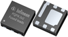
OptiMOS™ 6 power MOSFET 40 V in smallest form factor PQFN 2x2 package
With the new best-in-class OptiMOSTM 6 product family, Infineon offers a benchmark solution for efficiency in a small form factor, making it the perfect solution for applications such as wireless charging, load switches and low power DCDC applications. The small 4 mm2 footprint, combined with outstanding electrical performance contributes towards form factor improvement in end applications.
Summary of Features
Lowest RDS(on) with industries best FOMs in PQFN 2x2 package
Low package parasitics due to improved package design with clip
Superior thermal resistance for a PQFN 2x2 package
Ultra-small package for best form factor
Pulsed current capability up to 254 A
100% avalanche tested, Pb-free lead plating, RoHS compliant
Benefits
Optimized for highest performance and power density
Easy thermal management low conduction and switching losses
Form factor improvement offers cost savings
Small footprint facilitates optimal part placement on the PCB
High reliability and environmentally friendly
Potential Applications
Wireless charging
Charger
Robots & drones
Industrial SMPS
Server
Telecom
Consumer
OptiMOS™ 6 power MOSFET 40 V in smallest form factor PQFN 2x2 package
With the new best-in-class OptiMOSTM 6 product family, Infineon offers a benchmark solution for efficiency in a small form factor, making it the perfect solution for applications such as wireless charging, load switches and low power DCDC applications. The small 4 mm2 footprint, combined with outstanding electrical performance contributes towards form factor improvement in end applications.
Summary of Features
- Lowest RDS(on) with industries best FOMs in PQFN 2x2 package
- Low package parasitics due to improved package design with clip
- Superior thermal resistance for a PQFN 2x2 package
- Ultra-small package for best form factor
- Pulsed current capability up to 254 A
- 100% avalanche tested, Pb-free lead plating, RoHS compliant
Benefits
- Optimized for highest performance and power density
- Easy thermal management low conduction and switching losses
- Form factor improvement offers cost savings
- Small footprint facilitates optimal part placement on the PCB
- High reliability and environmentally friendly
Potential Applications
- Wireless charging
- Charger
- Robots & drones
- Industrial SMPS
- Server
- Telecom
- Consumer