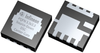
OptiMOS™ low-voltage power MOSFET 40 V in PQFN 3.3x3.3 Source-Down DSC package with industry leading RDS(on) and superior thermal performance
Infineon is presenting the new product of the portfolio extension for the innovative Source-Down technology: the OptiMOSTM 5 40 V PQFN 3.3x3.3 Source-Down: IQE013N04LM6CGSC. The revolutionary Source-Down technology introduces a flipped silicon die, which is positioned upside down inside of the components. This adjustment allows the source potential (instead of the drain potential) to be connected to the PCB over the thermal pad. Therefore, it offers several advantages, such as increased thermal capability, advanced power density or improved layout possibilities.
Furthermore, the higher efficiency, the reduced active cooling requirements and the effective layout for thermal management are benefits at the system level. Thanks to the new benchmark RDS(on) and the innovative layout capacities enable the Source-Down concept to have a leading position in temperature management.
Moreover, with the dual-side cooling package three times more power can be dissipated compared to the overmolded package. The Source-Down portfolio is addressing applications, such as drives, telecom, SMPS or server. The new technology can be found in two different footprints for now: Source-Down Standard-Gate and Source-Down Center-Gate (optimized for parallelization).
Summary of Features
Major reduction in RDS(on) by up to 30% compared to current technology
Improved RthJC over current PQFN package technology
Standard-gate and center-gate footprints available
New, optimized layout possibilities
Benefits
Enabling highest power density and performance
Superior thermal performance
Optimized layout possibilities for efficient use of real-estate
Simplifying parallel configuration of multiple MOSFETs with center-gate footprint
Improved PCB losses
Reduced parasitics
Potential Applications
Drives
SMPS
Server
Telecom
OR-ing
Battery management
Applications
48 V intermediate bus converter (IBC)
48 V to 12 V DC-DC converter
Automotive USB power delivery - Head unit
Cordless power tools and outdoor power equipment
DIN rail power supplies
Designers who used this product also designed with
XDPP1100-Q024 | Digital Power Controllers
BSZ070N08LS5 | N-Channel Power MOSFET
XDPP1100-Q024 | Digital Power Controllers
BSZ070N08LS5 | N-Channel Power MOSFET
XDPP1100-Q024 | Digital Power Controllers
BSZ070N08LS5 | N-Channel Power MOSFET
OptiMOS™ low-voltage power MOSFET 40 V in PQFN 3.3x3.3 Source-Down DSC package with industry leading RDS(on) and superior thermal performance
Infineon is presenting the new product of the portfolio extension for the innovative Source-Down technology: the OptiMOSTM 5 40 V PQFN 3.3x3.3 Source-Down: IQE013N04LM6CGSC. The revolutionary Source-Down technology introduces a flipped silicon die, which is positioned upside down inside of the components. This adjustment allows the source potential (instead of the drain potential) to be connected to the PCB over the thermal pad. Therefore, it offers several advantages, such as increased thermal capability, advanced power density or improved layout possibilities.
Furthermore, the higher efficiency, the reduced active cooling requirements and the effective layout for thermal management are benefits at the system level. Thanks to the new benchmark RDS(on) and the innovative layout capacities enable the Source-Down concept to have a leading position in temperature management.
Moreover, with the dual-side cooling package three times more power can be dissipated compared to the overmolded package. The Source-Down portfolio is addressing applications, such as drives, telecom, SMPS or server. The new technology can be found in two different footprints for now: Source-Down Standard-Gate and Source-Down Center-Gate (optimized for parallelization).
Summary of Features
- Major reduction in RDS(on) by up to 30% compared to current technology
- Improved RthJC over current PQFN package technology
- Standard-gate and center-gate footprints available
- New, optimized layout possibilities
Benefits
- Enabling highest power density and performance
- Superior thermal performance
- Optimized layout possibilities for efficient use of real-estate
- Simplifying parallel configuration of multiple MOSFETs with center-gate footprint
- Improved PCB losses
- Reduced parasitics
Potential Applications
- Drives
- SMPS
- Battery management
Applications
- 48 V intermediate bus converter (IBC)
- 48 V to 12 V DC-DC converter
- Automotive USB power delivery - Head unit
- Cordless power tools and outdoor power equipment
- DIN rail power supplies
Designers who used this product also designed with
- XDPP1100-Q024 |
Digital Power Controllers
- BSZ070N08LS5 |
N-Channel Power MOSFET
- XDPP1100-Q024 |
Digital Power Controllers
- BSZ070N08LS5 |
N-Channel Power MOSFET
- XDPP1100-Q024 |
Digital Power Controllers
- BSZ070N08LS5 |
N-Channel Power MOSFET