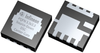
Infineon Technologies AG Power - MOSFET (Si/SiC) - N-Channel Power MOSFET - IQE008N03LM5CGSC IQE008N03LM5CGSC

Description
OptiMOS™ low-voltage power MOSFET 30 V in PQFN 3.3x3.3 Source-Down Center-Gate DSC package The IQE008N03LM5CGSC is part of the Source-Down family with RDS(on) of 0.85 mOhm. The Source-Down technology introduces a flipped silicon die, which is positioned upside down inside the components. It offers increased thermal capability, improved power density and layout possibilities. The dual-side cooling package dissipates three times more power than the overmolded package, and is available in Standard and Center-Gate footprints. Summary of Features Major reduction in RDS(on) by up to 30% Improved RthJC compared to PQFN packages Standard & Center-gate footprints New, optimized layout possibilities Benefits High power density and performance Superior thermal performance Efficient layout for space use Simplified MOSFET parallelization Improved PCB losses Reduced parasitics Potential Applications Drives SMPS Server Telecom Battery management
Request a Quote
Description
OptiMOS™ low-voltage power MOSFET 30 V in PQFN 3.3x3.3 Source-Down Center-Gate DSC package The IQE008N03LM5CGSC is part of the Source-Down family with RDS(on) of 0.85 mOhm. The Source-Down technology introduces a flipped silicon die, which is positioned upside down inside the components. It offers increased thermal capability, improved power density and layout possibilities. The dual-side cooling package dissipates three times more power than the overmolded package, and is available in Standard and Center-Gate footprints. Summary of Features Major reduction in RDS(on) by up to 30% Improved RthJC compared to PQFN packages Standard & Center-gate footprints New, optimized layout possibilities Benefits High power density and performance Superior thermal performance Efficient layout for space use Simplified MOSFET parallelization Improved PCB losses Reduced parasitics Potential Applications Drives SMPS Server Telecom Battery management
Request a Quote
Datasheet
Datasheet Summary
Powered by GS/AI

The IQE008N03LM5CGSC is a 30 V N-channel MOSFET designed for high-performance switch-mode power supplies, such as synchronous rectifiers. It is packaged in the PG-WHTFN-9 (PQFN 3.3x3.3 mm) case with source-down, center-gate mounting for improved thermal performance. The device has a maximum on-resistance of 0.85 mΩ at V_GS=4.5 V, a continuous drain current of 252 A, and a pulsed drain current of 1008 A. It is avalanche-tested and meets JEDEC industrial qualification standards. Thermal resistance from junction to case is 1.4 °C/W or 0.7 °C/W depending on the thermal path. The package is RoHS compliant and halogen-free according to IEC 61249-2-21.

Datasheet Summary
Powered by GS/AI

The IQE008N03LM5CGSC is a 30 V N-channel MOSFET designed for high-performance switch-mode power supplies, such as synchronous rectifiers. It is packaged in the PG-WHTFN-9 (PQFN 3.3x3.3 mm) case with source-down, center-gate mounting for improved thermal performance. The device has a maximum on-resistance of 0.85 mΩ at V_GS=4.5 V, a continuous drain current of 252 A, and a pulsed drain current of 1008 A. It is avalanche-tested and meets JEDEC industrial qualification standards. Thermal resistance from junction to case is 1.4 °C/W or 0.7 °C/W depending on the thermal path. The package is RoHS compliant and halogen-free according to IEC 61249-2-21.

Suppliers

Company
Product
Description
Supplier Links
Power - MOSFET (Si/SiC) - N-Channel Power MOSFET - IQE008N03LM5CGSC - IQE008N03LM5CGSC - Infineon Technologies AG
Neubiberg, Germany
Power - MOSFET (Si/SiC) - N-Channel Power MOSFET - IQE008N03LM5CGSC
IQE008N03LM5CGSC
Power - MOSFET (Si/SiC) - N-Channel Power MOSFET - IQE008N03LM5CGSC IQE008N03LM5CGSC
OptiMOS™ low-voltage power MOSFET 30 V in PQFN 3.3x3.3 Source-Down Center-Gate DSC package The IQE008N03LM5CGSC is part of the Source-Down family with RDS(on) of 0.85 mOhm. The Source-Down technology introduces a flipped silicon die, which is positioned upside down inside the components. It offers increased thermal capability, improved power density and layout possibilities. The dual-side cooling package dissipates three times more power than the overmolded package, and is available in Standard and Center-Gate footprints. Summary of Features Major reduction in RDS(on) by up to 30% Improved RthJC compared to PQFN packages Standard & Center-gate footprints New, optimized layout possibilities Benefits High power density and performance Superior thermal performance Efficient layout for space use Simplified MOSFET parallelization Improved PCB losses Reduced parasitics Potential Applications Drives SMPS Server Telecom Battery management

OptiMOS™ low-voltage power MOSFET 30 V in PQFN 3.3x3.3 Source-Down Center-Gate DSC package

The IQE008N03LM5CGSC is part of the Source-Down family with RDS(on) of 0.85 mOhm. The Source-Down technology introduces a flipped silicon die, which is positioned upside down inside the components.

It offers increased thermal capability, improved power density and layout possibilities. The dual-side cooling package dissipates three times more power than the overmolded package, and is available in Standard and Center-Gate footprints.


Summary of Features

  • Major reduction in RDS(on) by up to 30%
  • Improved RthJC compared to PQFN packages
  • Standard & Center-gate footprints
  • New, optimized layout possibilities

Benefits

  • High power density and performance
  • Superior thermal performance
  • Efficient layout for space use
  • Simplified MOSFET parallelization
  • Improved PCB losses
  • Reduced parasitics

Potential Applications

  • Drives
  • SMPS
    • Server
    • Telecom
  • Battery management
Supplier's Site Datasheet

Technical Specifications

  Infineon Technologies AG
Product Category Power MOSFET
Product Number IQE008N03LM5CGSC
Product Name Power - MOSFET (Si/SiC) - N-Channel Power MOSFET - IQE008N03LM5CGSC
Polarity N-Channel; N
Transistor Technology / Material Si/SiC
rDS(on) 8.50E-4 ohms
Unlock Full Specs
to access all available technical data