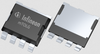
Infineon Technologies AG Power - MOSFET (Si/SiC) - N-Channel Power MOSFET - IPM018N10NM5LF2 IPM018N10NM5LF2

Description
OptiMOS™ 5 single N-channel Linear FET 2 100 V, 1.8 mΩ, 176 A in 8 mm x 8 mm footprint IPM018N10NM5LF2 is Infineon’s best-in-class OptiMOS™ 5 Linear FET 2 100 V in the new 8x8 mTOLG, offering the industry’s lowest RDS(on) and wide SOA at 25˚C. This is a JEDEC listed package, compatible with other 8x8 mm2 gullwing package MOSFETs, i.e. LFPAK88 type. The combination of the OptiMOS™ 5 Linear FET 2 technology and the mTOLG package, is designed to provide highest power density for inrush current protection applications such as hot-swap, e-fuse, and battery protection in battery management systems (BMS). Summary of Features 8 mm x 8 mm footprint Wide safe operating area (SOA) Ultra low On-Resistance Lower leakage current Optimized transfer characteristic Benefits Highest power density in 8x8 mm2 Low conduction losses Rugged linear mode operation Better current sharing Improved gate driver compatibility Applications Battery management systems (BMS) Server power supply units (PSU) Telecommunication infrastructure
Request a Quote Datasheet
Description
OptiMOS™ 5 single N-channel Linear FET 2 100 V, 1.8 mΩ, 176 A in 8 mm x 8 mm footprint IPM018N10NM5LF2 is Infineon’s best-in-class OptiMOS™ 5 Linear FET 2 100 V in the new 8x8 mTOLG, offering the industry’s lowest RDS(on) and wide SOA at 25˚C. This is a JEDEC listed package, compatible with other 8x8 mm2 gullwing package MOSFETs, i.e. LFPAK88 type. The combination of the OptiMOS™ 5 Linear FET 2 technology and the mTOLG package, is designed to provide highest power density for inrush current protection applications such as hot-swap, e-fuse, and battery protection in battery management systems (BMS). Summary of Features 8 mm x 8 mm footprint Wide safe operating area (SOA) Ultra low On-Resistance Lower leakage current Optimized transfer characteristic Benefits Highest power density in 8x8 mm2 Low conduction losses Rugged linear mode operation Better current sharing Improved gate driver compatibility Applications Battery management systems (BMS) Server power supply units (PSU) Telecommunication infrastructure
Request a Quote Datasheet

Suppliers

Company
Product
Description
Supplier Links
Power - MOSFET (Si/SiC) - N-Channel Power MOSFET - IPM018N10NM5LF2 - IPM018N10NM5LF2 - Infineon Technologies AG
Neubiberg, Germany
Power - MOSFET (Si/SiC) - N-Channel Power MOSFET - IPM018N10NM5LF2
IPM018N10NM5LF2
Power - MOSFET (Si/SiC) - N-Channel Power MOSFET - IPM018N10NM5LF2 IPM018N10NM5LF2
OptiMOS™ 5 single N-channel Linear FET 2 100 V, 1.8 mΩ, 176 A in 8 mm x 8 mm footprint IPM018N10NM5LF2 is Infineon’s best-in-class OptiMOS™ 5 Linear FET 2 100 V in the new 8x8 mTOLG, offering the industry’s lowest RDS(on) and wide SOA at 25˚C. This is a JEDEC listed package, compatible with other 8x8 mm2 gullwing package MOSFETs, i.e. LFPAK88 type. The combination of the OptiMOS™ 5 Linear FET 2 technology and the mTOLG package, is designed to provide highest power density for inrush current protection applications such as hot-swap, e-fuse, and battery protection in battery management systems (BMS). Summary of Features 8 mm x 8 mm footprint Wide safe operating area (SOA) Ultra low On-Resistance Lower leakage current Optimized transfer characteristic Benefits Highest power density in 8x8 mm2 Low conduction losses Rugged linear mode operation Better current sharing Improved gate driver compatibility Applications Battery management systems (BMS) Server power supply units (PSU) Telecommunication infrastructure

OptiMOS™ 5 single N-channel Linear FET 2 100 V, 1.8 mΩ, 176 A in 8 mm x 8 mm footprint

IPM018N10NM5LF2 is Infineon’s best-in-class OptiMOS™ 5 Linear FET 2 100 V in the new 8x8 mTOLG, offering the industry’s lowest RDS(on) and wide SOA at 25˚C. This is a JEDEC listed package, compatible with other 8x8 mm2 gullwing package MOSFETs, i.e. LFPAK88 type.

The combination of the OptiMOS™ 5 Linear FET 2 technology and the mTOLG package, is designed to provide highest power density for inrush current protection applications such as hot-swap, e-fuse, and battery protection in battery management systems (BMS).


Summary of Features

  • 8 mm x 8 mm footprint
  • Wide safe operating area (SOA)
  • Ultra low On-Resistance
  • Lower leakage current
  • Optimized transfer characteristic

Benefits

  • Highest power density in 8x8 mm2
  • Low conduction losses
  • Rugged linear mode operation
  • Better current sharing
  • Improved gate driver compatibility

Applications

  • Battery management systems (BMS)
  • Server power supply units (PSU)
  • Telecommunication infrastructure
Supplier's Site Datasheet

Technical Specifications

  Infineon Technologies AG
Product Category Power MOSFET
Product Number IPM018N10NM5LF2
Product Name Power - MOSFET (Si/SiC) - N-Channel Power MOSFET - IPM018N10NM5LF2
Polarity N-Channel; N
Transistor Technology / Material Si/SiC
rDS(on) 0.0019 ohms
Unlock Full Specs
to access all available technical data