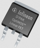
Infineon Technologies AG N-Channel Power MOSFET IPB110N20N3LF

Description
Combining a low RDS(on) with a wide safe operating area (SOA) OptiMOS™ Linear FET is a revolutionary approach to avoid the trade-off between on-state resistance (R DS(on)) and linear mode capability – operation in the saturation region of an enhanced mode MOSFET. It offers the state-of-the-art R DS(on) of a trench MOSFET together with the wide safe operating area of a classic planar MOSFET. Summary of Features Combination of low R DS(on) and wide safe operating area (SOA) High max. pulse current High continuous pulse current Benefits Rugged linear mode operation Low conduction losses Higher in-rush current enabled for faster start-up and shorter down time Potential Applications Telecom Battery management Applications Energy Storage Systems Space applications Designers who used this product also designed with CY15B102Q-SXET | F-RAM (Ferroelectric RAM) IAUC90N10S5N062 | Automotive MOSFET BSC007N04LS6 | N-Channel Power MOSFET IAUC120N04S6N006 | Automotive MOSFET CY15B102Q-SXET | F-RAM (Ferroelectric RAM) IAUC90N10S5N062 | Automotive MOSFET BSC007N04LS6 | N-Channel Power MOSFET IAUC120N04S6N006 | Automotive MOSFET CY15B102Q-SXET | F-RAM (Ferroelectric RAM) IAUC90N10S5N062 | Automotive MOSFET BSC007N04LS6 | N-Channel Power MOSFET IAUC120N04S6N006 | Automotive MOSFET
Request a Quote
Datasheet
Datasheet Summary
Powered by GS/AI

The IPB110N20N3LF is an N-channel MOSFET designed for hot-swap and e-fuse applications, featuring a drain-source breakdown voltage of 200 V, a maximum on-state resistance of 11 mΩ at 10 V gate-source voltage, and a continuous drain current of 88 A. It is packaged in a PG-TO263-3 case with a maximum power dissipation of 250 W at 25°C case temperature. The device is qualified according to JEDEC standards, is RoHS compliant, and halogen-free per IEC61249-2-21. It offers a wide safe operating area and is 100% avalanche tested with single-pulse avalanche energy up to 560 mJ.

Suppliers

Company
Product
Description
Supplier Links
N-Channel Power MOSFET - IPB110N20N3LF - Infineon Technologies AG
Neubiberg, Germany
N-Channel Power MOSFET
IPB110N20N3LF
N-Channel Power MOSFET IPB110N20N3LF
Combining a low RDS(on) with a wide safe operating area (SOA) OptiMOS™ Linear FET is a revolutionary approach to avoid the trade-off between on-state resistance (R DS(on)) and linear mode capability – operation in the saturation region of an enhanced mode MOSFET. It offers the state-of-the-art R DS(on) of a trench MOSFET together with the wide safe operating area of a classic planar MOSFET. Summary of Features Combination of low R DS(on) and wide safe operating area (SOA) High max. pulse current High continuous pulse current Benefits Rugged linear mode operation Low conduction losses Higher in-rush current enabled for faster start-up and shorter down time Potential Applications Telecom Battery management Applications Energy Storage Systems Space applications Designers who used this product also designed with CY15B102Q-SXET | F-RAM (Ferroelectric RAM) IAUC90N10S5N062 | Automotive MOSFET BSC007N04LS6 | N-Channel Power MOSFET IAUC120N04S6N006 | Automotive MOSFET CY15B102Q-SXET | F-RAM (Ferroelectric RAM) IAUC90N10S5N062 | Automotive MOSFET BSC007N04LS6 | N-Channel Power MOSFET IAUC120N04S6N006 | Automotive MOSFET CY15B102Q-SXET | F-RAM (Ferroelectric RAM) IAUC90N10S5N062 | Automotive MOSFET BSC007N04LS6 | N-Channel Power MOSFET IAUC120N04S6N006 | Automotive MOSFET

Combining a low RDS(on) with a wide safe operating area (SOA)

OptiMOS™ Linear FET is a revolutionary approach to avoid the trade-off between on-state resistance (R DS(on)) and linear mode capability – operation in the saturation region of an enhanced mode MOSFET. It offers the state-of-the-art R DS(on) of a trench MOSFET together with the wide safe operating area of a classic planar MOSFET.


Summary of Features

  • Combination of low R DS(on) and wide safe operating area (SOA)
  • High max. pulse current
  • High continuous pulse current

Benefits

  • Rugged linear mode operation
  • Low conduction losses
  • Higher in-rush current enabled for faster start-up and shorter down time

Potential Applications

  • Telecom
  • Battery management

Applications

  • Energy Storage Systems
  • Space applications

Designers who used this product also designed with


  • CY15B102Q-SXET |
    F-RAM (Ferroelectric RAM)
  • IAUC90N10S5N062 |
    Automotive MOSFET
  • BSC007N04LS6 |
    N-Channel Power MOSFET
  • IAUC120N04S6N006 |
    Automotive MOSFET
  • CY15B102Q-SXET |
    F-RAM (Ferroelectric RAM)
  • IAUC90N10S5N062 |
    Automotive MOSFET
  • BSC007N04LS6 |
    N-Channel Power MOSFET
  • IAUC120N04S6N006 |
    Automotive MOSFET
  • CY15B102Q-SXET |
    F-RAM (Ferroelectric RAM)
  • IAUC90N10S5N062 |
    Automotive MOSFET
  • BSC007N04LS6 |
    N-Channel Power MOSFET
  • IAUC120N04S6N006 |
    Automotive MOSFET
Supplier's Site Datasheet
Transistors IPB110N20N3LF
TO-263-3 MOSFETs ROHS

TO-263-3 MOSFETs ROHS

Supplier's Site

Technical Specifications

  Infineon Technologies AG ODG (Origin Data Global)
Product Category Power MOSFET Transistors
Product Number IPB110N20N3LF IPB110N20N3LF
Product Name N-Channel Power MOSFET Transistors
Polarity N-Channel; N
Transistor Technology / Material Si/SiC
rDS(on) 0.0110 ohms
Unlock Full Specs
to access all available technical data