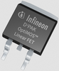
Infineon Technologies AG N-Channel Power MOSFET IPB048N15N5LF

Description
Combining a low RDS(on) with a wide safe operating area (SOA) OptiMOS™ Linear FET is a revolutionary approach to avoid the trade-off between on-state resistance (R DS(on)) and linear mode capability – operation in the saturation region of an enhanced mode MOSFET. It offers the state-of-the-art R DS(on) of a trench MOSFET together with the wide safe operating area of a classic planar MOSFET. Summary of Features Combination of low R DS(on) and wide safe operating area (SOA) High max. pulse current High continuous pulse current Benefits Rugged linear mode operation Low conduction losses Higher in-rush current enabled for faster start-up and shorter down time Potential Applications Telecom Battery management Applications Telecommunication infrastructure Uninterruptible power supplies (UPS) Wireless Communication Designers who used this product also designed with S25HS02GTDPBHV150 | SEMPER™ NOR flash BAS40-06 | Schottky Diodes 2EDF7275K | Gate driver ICs BSS138N | Small signal/small power MOSFET S25HS02GTDPBHV150 | SEMPER™ NOR flash BAS40-06 | Schottky Diodes 2EDF7275K | Gate driver ICs BSS138N | Small signal/small power MOSFET S25HS02GTDPBHV150 | SEMPER™ NOR flash BAS40-06 | Schottky Diodes 2EDF7275K | Gate driver ICs BSS138N | Small signal/small power MOSFET
Request a Quote
Datasheet
Datasheet Summary
Powered by GS/AI

The IPB048N15N5LF is a 150 V N-channel MOSFET in a PG-TO263-3 package, designed for hot-swap and e-fuse applications. It features a maximum on-state resistance of 4.8 mΩ at 10 V gate voltage and supports a continuous drain current of 150 A at 25 °C case temperature. The device has a safe operating area optimized for linear mode operation, is 100% avalanche tested, and meets RoHS and IEC 61249-2-21 halogen-free requirements. Its gate-source voltage range is −20 V to +20 V, and it operates with a junction temperature range of −55 °C to 150 °C.

Suppliers

Company
Product
Description
Supplier Links
N-Channel Power MOSFET - IPB048N15N5LF - Infineon Technologies AG
Neubiberg, Germany
N-Channel Power MOSFET
IPB048N15N5LF
N-Channel Power MOSFET IPB048N15N5LF
Combining a low RDS(on) with a wide safe operating area (SOA) OptiMOS™ Linear FET is a revolutionary approach to avoid the trade-off between on-state resistance (R DS(on)) and linear mode capability – operation in the saturation region of an enhanced mode MOSFET. It offers the state-of-the-art R DS(on) of a trench MOSFET together with the wide safe operating area of a classic planar MOSFET. Summary of Features Combination of low R DS(on) and wide safe operating area (SOA) High max. pulse current High continuous pulse current Benefits Rugged linear mode operation Low conduction losses Higher in-rush current enabled for faster start-up and shorter down time Potential Applications Telecom Battery management Applications Telecommunication infrastructure Uninterruptible power supplies (UPS) Wireless Communication Designers who used this product also designed with S25HS02GTDPBHV150 | SEMPER™ NOR flash BAS40-06 | Schottky Diodes 2EDF7275K | Gate driver ICs BSS138N | Small signal/small power MOSFET S25HS02GTDPBHV150 | SEMPER™ NOR flash BAS40-06 | Schottky Diodes 2EDF7275K | Gate driver ICs BSS138N | Small signal/small power MOSFET S25HS02GTDPBHV150 | SEMPER™ NOR flash BAS40-06 | Schottky Diodes 2EDF7275K | Gate driver ICs BSS138N | Small signal/small power MOSFET

Combining a low RDS(on) with a wide safe operating area (SOA)

OptiMOS™ Linear FET is a revolutionary approach to avoid the trade-off between on-state resistance (R DS(on)) and linear mode capability – operation in the saturation region of an enhanced mode MOSFET. It offers the state-of-the-art R DS(on) of a trench MOSFET together with the wide safe operating area of a classic planar MOSFET.


Summary of Features

  • Combination of low R DS(on) and wide safe operating area (SOA)
  • High max. pulse current
  • High continuous pulse current

Benefits

  • Rugged linear mode operation
  • Low conduction losses
  • Higher in-rush current enabled for faster start-up and shorter down time

Potential Applications

  • Telecom
  • Battery management

Applications

  • Telecommunication infrastructure
  • Uninterruptible power supplies (UPS)
  • Wireless Communication

Designers who used this product also designed with


  • S25HS02GTDPBHV150 |
    SEMPER™ NOR flash
  • BAS40-06 |
    Schottky Diodes
  • 2EDF7275K |
    Gate driver ICs
  • BSS138N |
    Small signal/small power MOSFET
  • S25HS02GTDPBHV150 |
    SEMPER™ NOR flash
  • BAS40-06 |
    Schottky Diodes
  • 2EDF7275K |
    Gate driver ICs
  • BSS138N |
    Small signal/small power MOSFET
  • S25HS02GTDPBHV150 |
    SEMPER™ NOR flash
  • BAS40-06 |
    Schottky Diodes
  • 2EDF7275K |
    Gate driver ICs
  • BSS138N |
    Small signal/small power MOSFET
Supplier's Site Datasheet

Technical Specifications

  Infineon Technologies AG
Product Category Power MOSFET
Product Number IPB048N15N5LF
Product Name N-Channel Power MOSFET
Polarity N-Channel; N
Transistor Technology / Material Si/SiC
rDS(on) 0.0048 ohms
Unlock Full Specs
to access all available technical data