
Infineon Technologies AG N-Channel Power MOSFET BSG0811ND

Description
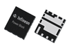
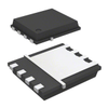
OptiMOS™ 5 Power Block is a leadless SMD package in a 5.0x6.0mm² package outline, including a low-side and a high-side MOSFET in a synchronous buck converter configuration. By replacing two separate discrete packages, such as SO8 or SuperSO8, with the OptiMOS™ 5 Power Block, customers can shrink their designs up to 85%. Standardizing power packages benefits the customer, as the number of different package outlines available in the market place is minimized. Summary of Features 50A max average load current Source-down low side MOSFET for better PCB cooling Internally connected low-side and high side (lowest loop inductance) High side Kelvin connection for more efficient driving Benefits Compact and simplified layout for a DC-DC converter Optimized layout with lowest loop inductivity and best thermal performance Potential Applications Desktop and server Single-phase & multiphase POL CPU/GPU regulation in notebooks & DDR memory High power density voltage regulator Applications Space applications Designers who used this product also designed with ISZ230N10NM6 | N-Channel Power MOSFET BSC117N08NS5 | N-Channel Power MOSFET IPB110N20N3LF | N-Channel Power MOSFET CY15B102Q-SXET | F-RAM (Ferroelectric RAM) ISZ230N10NM6 | N-Channel Power MOSFET BSC117N08NS5 | N-Channel Power MOSFET IPB110N20N3LF | N-Channel Power MOSFET CY15B102Q-SXET | F-RAM (Ferroelectric RAM) ISZ230N10NM6 | N-Channel Power MOSFET BSC117N08NS5 | N-Channel Power MOSFET IPB110N20N3LF | N-Channel Power MOSFET CY15B102Q-SXET | F-RAM (Ferroelectric RAM)
Request a Quote Datasheet
Description
OptiMOS™ 5 Power Block is a leadless SMD package in a 5.0x6.0mm² package outline, including a low-side and a high-side MOSFET in a synchronous buck converter configuration. By replacing two separate discrete packages, such as SO8 or SuperSO8, with the OptiMOS™ 5 Power Block, customers can shrink their designs up to 85%. Standardizing power packages benefits the customer, as the number of different package outlines available in the market place is minimized. Summary of Features 50A max average load current Source-down low side MOSFET for better PCB cooling Internally connected low-side and high side (lowest loop inductance) High side Kelvin connection for more efficient driving Benefits Compact and simplified layout for a DC-DC converter Optimized layout with lowest loop inductivity and best thermal performance Potential Applications Desktop and server Single-phase & multiphase POL CPU/GPU regulation in notebooks & DDR memory High power density voltage regulator Applications Space applications Designers who used this product also designed with ISZ230N10NM6 | N-Channel Power MOSFET BSC117N08NS5 | N-Channel Power MOSFET IPB110N20N3LF | N-Channel Power MOSFET CY15B102Q-SXET | F-RAM (Ferroelectric RAM) ISZ230N10NM6 | N-Channel Power MOSFET BSC117N08NS5 | N-Channel Power MOSFET IPB110N20N3LF | N-Channel Power MOSFET CY15B102Q-SXET | F-RAM (Ferroelectric RAM) ISZ230N10NM6 | N-Channel Power MOSFET BSC117N08NS5 | N-Channel Power MOSFET IPB110N20N3LF | N-Channel Power MOSFET CY15B102Q-SXET | F-RAM (Ferroelectric RAM)
Request a Quote Datasheet

Suppliers

Company
Product
Description
Supplier Links
N-Channel Power MOSFET - BSG0811ND - Infineon Technologies AG
Neubiberg, Germany
N-Channel Power MOSFET
BSG0811ND
N-Channel Power MOSFET BSG0811ND
OptiMOS™ 5 Power Block is a leadless SMD package in a 5.0x6.0mm² package outline, including a low-side and a high-side MOSFET in a synchronous buck converter configuration. By replacing two separate discrete packages, such as SO8 or SuperSO8, with the OptiMOS™ 5 Power Block, customers can shrink their designs up to 85%. Standardizing power packages benefits the customer, as the number of different package outlines available in the market place is minimized. Summary of Features 50A max average load current Source-down low side MOSFET for better PCB cooling Internally connected low-side and high side (lowest loop inductance) High side Kelvin connection for more efficient driving Benefits Compact and simplified layout for a DC-DC converter Optimized layout with lowest loop inductivity and best thermal performance Potential Applications Desktop and server Single-phase & multiphase POL CPU/GPU regulation in notebooks & DDR memory High power density voltage regulator Applications Space applications Designers who used this product also designed with ISZ230N10NM6 | N-Channel Power MOSFET BSC117N08NS5 | N-Channel Power MOSFET IPB110N20N3LF | N-Channel Power MOSFET CY15B102Q-SXET | F-RAM (Ferroelectric RAM) ISZ230N10NM6 | N-Channel Power MOSFET BSC117N08NS5 | N-Channel Power MOSFET IPB110N20N3LF | N-Channel Power MOSFET CY15B102Q-SXET | F-RAM (Ferroelectric RAM) ISZ230N10NM6 | N-Channel Power MOSFET BSC117N08NS5 | N-Channel Power MOSFET IPB110N20N3LF | N-Channel Power MOSFET CY15B102Q-SXET | F-RAM (Ferroelectric RAM)

OptiMOS™ 5 Power Block is a leadless SMD package in a 5.0x6.0mm² package outline, including a low-side and a high-side MOSFET in a synchronous buck converter configuration. By replacing two separate discrete packages, such as SO8 or SuperSO8, with the OptiMOS™ 5 Power Block, customers can shrink their designs up to 85%. Standardizing power packages benefits the customer, as the number of different package outlines available in the market place is minimized.


Summary of Features

  • 50A max average load current
  • Source-down low side MOSFET for better PCB cooling
  • Internally connected low-side and high side (lowest loop inductance)
  • High side Kelvin connection for more efficient driving

Benefits

  • Compact and simplified layout for a DC-DC converter
  • Optimized layout with lowest loop inductivity and best thermal performance

Potential Applications

  • Desktop and server
  • Single-phase & multiphase POL
  • CPU/GPU regulation in notebooks & DDR memory
  • High power density voltage regulator

Applications

  • Space applications

Designers who used this product also designed with


  • ISZ230N10NM6 |
    N-Channel Power MOSFET
  • BSC117N08NS5 |
    N-Channel Power MOSFET
  • IPB110N20N3LF |
    N-Channel Power MOSFET
  • CY15B102Q-SXET |
    F-RAM (Ferroelectric RAM)
  • ISZ230N10NM6 |
    N-Channel Power MOSFET
  • BSC117N08NS5 |
    N-Channel Power MOSFET
  • IPB110N20N3LF |
    N-Channel Power MOSFET
  • CY15B102Q-SXET |
    F-RAM (Ferroelectric RAM)
  • ISZ230N10NM6 |
    N-Channel Power MOSFET
  • BSC117N08NS5 |
    N-Channel Power MOSFET
  • IPB110N20N3LF |
    N-Channel Power MOSFET
  • CY15B102Q-SXET |
    F-RAM (Ferroelectric RAM)
Supplier's Site Datasheet
TRANSISTORS - Transistors - FETs, MOSFETs - RF - BSG0811ND - 201401-BSG0811ND - Win Source Electronics
Laguna Hills, CA, United States
TRANSISTORS - Transistors - FETs, MOSFETs - RF - BSG0811ND
201401-BSG0811ND
TRANSISTORS - Transistors - FETs, MOSFETs - RF - BSG0811ND 201401-BSG0811ND
Manufacturer: Infineon Technologies Win Source Part Number: 201401-BSG0811ND Packaging: Reel - TR Mounting: SMD (SMT) FET Type: 2 N-Channel (Dual) Asymmetrical FET Feature: Logic Level Gate, 4.5V Drive Family Name: BSG0811ND Categories: Discrete Semiconductor Products Status: Active Temperature Range - Operating: -55°C to 150°C (TJ) Case / Package: PG-TISON-8 Maximum Power Dissipation: 2.5W Drain-Source Breakdown Voltage: 25V Continuous Drain Current at 25°C: 19A, 41A Gate-Source Threshold Voltage: 2V @ 250μA Max Gate Charge: 8.4nC @ 4.5V Max Input Capacitance: 1100pF @ 12V Maximum Rds On at Id,Vgs: 3 mOhm @ 20A, 10V ECCN: EAR99 Country of Origin: Malaysia Estimated EOL Date: 2029 Halogen Free: Compliant Is this a common-used part?: Yes Popularity: High Fake Threat In the Open Market: 50 pct. Supply and Demand Status: Limited

Manufacturer: Infineon Technologies
Win Source Part Number: 201401-BSG0811ND
Packaging: Reel - TR
Mounting: SMD (SMT)
FET Type: 2 N-Channel (Dual) Asymmetrical
FET Feature: Logic Level Gate, 4.5V Drive
Family Name: BSG0811ND
Categories: Discrete Semiconductor Products
Status: Active
Temperature Range - Operating: -55°C to 150°C (TJ)
Case / Package: PG-TISON-8
Maximum Power Dissipation: 2.5W
Drain-Source Breakdown Voltage: 25V
Continuous Drain Current at 25°C: 19A, 41A
Gate-Source Threshold Voltage: 2V @ 250μA
Max Gate Charge: 8.4nC @ 4.5V
Max Input Capacitance: 1100pF @ 12V
Maximum Rds On at Id,Vgs: 3 mOhm @ 20A, 10V
ECCN: EAR99
Country of Origin: Malaysia
Estimated EOL Date: 2029
Halogen Free: Compliant
Is this a common-used part?: Yes
Popularity: High
Fake Threat In the Open Market: 50 pct.
Supply and Demand Status: Limited

Buy Now Datasheet
Transistors - BSG0811ND - ODG (Origin Data Global)
Shenzhen, China
Transistors
BSG0811ND
Transistors BSG0811ND
MOSFET TRENCH <= 40V

MOSFET TRENCH <= 40V

Supplier's Site Datasheet
Singapore
40V MOSFET Transistor
2088-BSG0811ND
40V MOSFET Transistor 2088-BSG0811ND
MOSFETs TRENCH <= 40V Product overview: BSG0811ND from Infineon Technologies is a MOSFET Transistor for power switching, load control, motor drives, DC-DC converters, battery systems, and board-level power design. It is useful for engineers and buyers comparing datasheets, replacement parts, BOM lines, package options, lifecycle status, and procurement availability. Key searchable attributes include 40V. Search-friendly keywords include MOSFET, power transistor, switching, N-channel, P-channel, 40V, MOSFET Transistor, FETs, MOSFETs. This listing supports clearer product discovery for industrial, commercial, repair, automation, power, sensing, and embedded system projects. Product number 2088-BSG0811ND can be used for catalog matching and distributor lookup.

MOSFETs TRENCH <= 40V Product overview: BSG0811ND from Infineon Technologies is a MOSFET Transistor for power switching, load control, motor drives, DC-DC converters, battery systems, and board-level power design. It is useful for engineers and buyers comparing datasheets, replacement parts, BOM lines, package options, lifecycle status, and procurement availability. Key searchable attributes include 40V. Search-friendly keywords include MOSFET, power transistor, switching, N-channel, P-channel, 40V, MOSFET Transistor, FETs, MOSFETs. This listing supports clearer product discovery for industrial, commercial, repair, automation, power, sensing, and embedded system projects. Product number 2088-BSG0811ND can be used for catalog matching and distributor lookup.

Supplier's Site Datasheet
Sheung Wan, Hong Kong
MOSFET DIFFERENTIATED MOSFETS

MOSFET DIFFERENTIATED MOSFETS

Buy Now Datasheet

Technical Specifications

  Infineon Technologies AG Win Source Electronics ODG (Origin Data Global) ERSAELECTRONICS PTE. LTD. VAST STOCK CO., LIMITED
Product Category Power MOSFET Metal-Oxide Semiconductor FET (MOSFET) Transistors Metal-Oxide Semiconductor FET (MOSFET) Metal-Oxide Semiconductor FET (MOSFET)
Product Number BSG0811ND 201401-BSG0811ND BSG0811ND 2088-BSG0811ND BSG0811ND
Product Name N-Channel Power MOSFET TRANSISTORS - Transistors - FETs, MOSFETs - RF - BSG0811ND Transistors 40V MOSFET Transistor MOSFET
Polarity N-Channel; N+N N-Channel N-Channel
Transistor Technology / Material Si/SiC
rDS(on) 8.00E-4 to 0.0030 ohms
TJ -55 to 150 C (-67 to 302 F) -55 to 150 C (-67 to 302 F)
Package Type PG-TISON-8 SOT3; PG-TISON-8 Reel
Unlock Full Specs
to access all available technical data
