Infineon Technologies AG RF, Antenna centric solutions BGSX33M5U16

Description
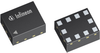
3P3T MIPI 2.1 antenna cross switch The BGSX33M5U16 RF CMOS switch is specifically designed for LTE and 5G antenna applications. This 3P3T cross-switch offers low insertion loss and low harmonic generation. The switch is controlled via a MIPI RFFE control interface. The on-chip controller allows power-supply voltages from 1.65 to1.95 V. Unlike GaAs technology, external DC blocking capacitors at the RF ports are only required if DC voltage is applied externally. The device has a very small size of only 2.0 mm x 2.0 mm and a thickness of 0.6 mm. Summary of Features High linearity up to 38 dBm peak power Fast switching time (max 2 µs) for 5G SRS applications Low insertion loss and high port to port isolation up to 7.125 GHz Enhanced isolation mode Low power consumption allows supply VIO MIPI RFFE 2.1 control interface Software and hardware programmable USID RoHS and WEEE compliant package Potential Applications Triple antenna routing/swapping for cellular mobile devices Triple antenna routing/swapping for 5G SRS application GSM, WCDMA, LTE and 5G FR1 frequency band applications 4x4 MIMO applications SAR reduction
Request a Quote Datasheet
Description
3P3T MIPI 2.1 antenna cross switch The BGSX33M5U16 RF CMOS switch is specifically designed for LTE and 5G antenna applications. This 3P3T cross-switch offers low insertion loss and low harmonic generation. The switch is controlled via a MIPI RFFE control interface. The on-chip controller allows power-supply voltages from 1.65 to1.95 V. Unlike GaAs technology, external DC blocking capacitors at the RF ports are only required if DC voltage is applied externally. The device has a very small size of only 2.0 mm x 2.0 mm and a thickness of 0.6 mm. Summary of Features High linearity up to 38 dBm peak power Fast switching time (max 2 µs) for 5G SRS applications Low insertion loss and high port to port isolation up to 7.125 GHz Enhanced isolation mode Low power consumption allows supply VIO MIPI RFFE 2.1 control interface Software and hardware programmable USID RoHS and WEEE compliant package Potential Applications Triple antenna routing/swapping for cellular mobile devices Triple antenna routing/swapping for 5G SRS application GSM, WCDMA, LTE and 5G FR1 frequency band applications 4x4 MIMO applications SAR reduction
Request a Quote Datasheet

Suppliers

Company
Product
Description
Supplier Links
RF, Antenna centric solutions - BGSX33M5U16 - Infineon Technologies AG
Neubiberg, Germany
RF, Antenna centric solutions
BGSX33M5U16
RF, Antenna centric solutions BGSX33M5U16
3P3T MIPI 2.1 antenna cross switch The BGSX33M5U16 RF CMOS switch is specifically designed for LTE and 5G antenna applications. This 3P3T cross-switch offers low insertion loss and low harmonic generation. The switch is controlled via a MIPI RFFE control interface. The on-chip controller allows power-supply voltages from 1.65 to1.95 V. Unlike GaAs technology, external DC blocking capacitors at the RF ports are only required if DC voltage is applied externally. The device has a very small size of only 2.0 mm x 2.0 mm and a thickness of 0.6 mm. Summary of Features High linearity up to 38 dBm peak power Fast switching time (max 2 µs) for 5G SRS applications Low insertion loss and high port to port isolation up to 7.125 GHz Enhanced isolation mode Low power consumption allows supply VIO MIPI RFFE 2.1 control interface Software and hardware programmable USID RoHS and WEEE compliant package Potential Applications Triple antenna routing/swapping for cellular mobile devices Triple antenna routing/swapping for 5G SRS application GSM, WCDMA, LTE and 5G FR1 frequency band applications 4x4 MIMO applications SAR reduction

3P3T MIPI 2.1 antenna cross switch

The BGSX33M5U16 RF CMOS switch is specifically designed for LTE and 5G antenna applications. This 3P3T cross-switch offers low insertion loss and low harmonic generation.

The switch is controlled via a MIPI RFFE control interface. The on-chip controller allows power-supply voltages from 1.65 to1.95 V. Unlike GaAs technology, external DC blocking capacitors at the RF ports are only required if DC voltage is applied externally. The device has a very small size of only 2.0 mm x 2.0 mm and a thickness of 0.6 mm.


Summary of Features

  • High linearity up to 38 dBm peak power
  • Fast switching time (max 2 µs) for 5G SRS applications
  • Low insertion loss and high port to port isolation up to 7.125 GHz
  • Enhanced isolation mode
  • Low power consumption allows supply VIO
  • MIPI RFFE 2.1 control interface
  • Software and hardware programmable USID
  • RoHS and WEEE compliant package

Potential Applications

  • Triple antenna routing/swapping for cellular mobile devices
  • Triple antenna routing/swapping for 5G SRS application
  • GSM, WCDMA, LTE and 5G FR1 frequency band applications
  • 4x4 MIMO applications
  • SAR reduction
Supplier's Site Datasheet

Technical Specifications

  Infineon Technologies AG
Product Category Antennas
Product Number BGSX33M5U16
Product Name RF, Antenna centric solutions
Primary Frequency Range 400.0 to 7125.0 MHz
Unlock Full Specs
to access all available technical data

Similar Products

RF, Antenna centric solutions - BGSA12GN10 - Infineon Technologies AG
Specs
Primary Frequency Range 100.0 to 6000.0 MHz
View Details
RF, Antenna centric solutions - BGSX44MU18 - Infineon Technologies AG
Specs
Primary Frequency Range 400.0 to 7125.0 MHz
View Details
RF, Antenna centric solutions - BGSA400ML10 - Infineon Technologies AG
Specs
Primary Frequency Range 400.0 to 7125.0 MHz
View Details
RF, Antenna centric solutions - BGSA142GN12 - Infineon Technologies AG
Specs
Primary Frequency Range 400.0 to 6000.0 MHz
View Details