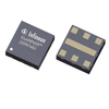
Infineon Technologies AG Gate Driver ICs 2ED21844S06J

Description
650 V, 2.5 A high current half-bridge gate driver IC with integrated bootstrap diode and shutdown in DSO-14 package 650 V half-bridge high current, and high speed gate driver for MOSFETand IGBT, with typical 2.5 A sink and source current in DSO-14 package. The smaller DSO-8 package version is also available: 2ED2184S06F. Based on Infineon’s SOI-technology, having excellent ruggedness and noise immunity against negative transient voltages on VS pin. No parasitic thyristor structures present in the device, hence no parasitic latch up at all temperature and voltage conditions. Summary of Features Operating voltages (VS node) upto + 650 V Negative VS transient immunity of 100 V Integrated ultra-fast, low resistance bootstrap diode, lower the BOM cost High and Low Voltage Pins Separated for Maximum Creepage and Clearance Separate logic and power ground Floating channel designed for bootstrap operation Integrated shoot-through protection with built-in dead time (programmable deadtime) Maximum supply voltage of 25 V Independent under voltage lockout (UVLO) for both channels 200 ns propagation delay IN, /SD input logic, Shutdown input turns off both channels Logic Operational up to –11 V on VS Pin Negative Voltage Tolerance On Inputs of –5 V The floating channel can be used to drive an N-channel MOSFET, SiC MOSFET or IGBT in the high side configuration Benefits High current gate driver - suitable for high current power device, and high frequency application Integrated bootstrap diode (BSD) - Space saving, reduced BOM cost, smaller PCB at lower cost with simpler design 50% lower level-shift losses Excellent ruggedness and noise immunity against negative transient voltages (-100 V) on VS pin Applications EV charging Home appliances Industrial robots system solutions for Industry 4.0 Light electric vehicles (LEV) Smart induction cooktop – precise and efficient heating control Find our Variations for 2ED21844S06J Part No Package Input logic Interlock Deadtime 2ED2181S06F DSO - 8 HIN, LIN No None 2ED21814S06J DSO - 14 HIN, LIN No None 2ED2182S06F DSO - 8 HIN, LIN Yes Internal 400 ns 2ED21824S06J DSO - 14 HIN, LIN Yes Programmable 400 ns - 5000 ns 2ED2183S06F DSO - 8 HIN, /LIN Yes Internal 400 ns 2ED21834S06J DSO – 14 HIN, /LIN Yes Programmable 400 ns - 5000 ns 2ED2184S06F DSO - 8 IN, /SD Yes Internal 400 ns Part No Package Input logic Interlock Deadtime Designers who used this product also designed with IPD079N06L3 G | N-Channel Power MOSFET FF600R12KE7 | IGBT modules IPD079N06L3 G | N-Channel Power MOSFET FF600R12KE7 | IGBT modules IPD079N06L3 G | N-Channel Power MOSFET FF600R12KE7 | IGBT modules
Request a Quote Datasheet
Description
650 V, 2.5 A high current half-bridge gate driver IC with integrated bootstrap diode and shutdown in DSO-14 package 650 V half-bridge high current, and high speed gate driver for MOSFETand IGBT, with typical 2.5 A sink and source current in DSO-14 package. The smaller DSO-8 package version is also available: 2ED2184S06F. Based on Infineon’s SOI-technology, having excellent ruggedness and noise immunity against negative transient voltages on VS pin. No parasitic thyristor structures present in the device, hence no parasitic latch up at all temperature and voltage conditions. Summary of Features Operating voltages (VS node) upto + 650 V Negative VS transient immunity of 100 V Integrated ultra-fast, low resistance bootstrap diode, lower the BOM cost High and Low Voltage Pins Separated for Maximum Creepage and Clearance Separate logic and power ground Floating channel designed for bootstrap operation Integrated shoot-through protection with built-in dead time (programmable deadtime) Maximum supply voltage of 25 V Independent under voltage lockout (UVLO) for both channels 200 ns propagation delay IN, /SD input logic, Shutdown input turns off both channels Logic Operational up to –11 V on VS Pin Negative Voltage Tolerance On Inputs of –5 V The floating channel can be used to drive an N-channel MOSFET, SiC MOSFET or IGBT in the high side configuration Benefits High current gate driver - suitable for high current power device, and high frequency application Integrated bootstrap diode (BSD) - Space saving, reduced BOM cost, smaller PCB at lower cost with simpler design 50% lower level-shift losses Excellent ruggedness and noise immunity against negative transient voltages (-100 V) on VS pin Applications EV charging Home appliances Industrial robots system solutions for Industry 4.0 Light electric vehicles (LEV) Smart induction cooktop – precise and efficient heating control Find our Variations for 2ED21844S06J Part No Package Input logic Interlock Deadtime 2ED2181S06F DSO - 8 HIN, LIN No None 2ED21814S06J DSO - 14 HIN, LIN No None 2ED2182S06F DSO - 8 HIN, LIN Yes Internal 400 ns 2ED21824S06J DSO - 14 HIN, LIN Yes Programmable 400 ns - 5000 ns 2ED2183S06F DSO - 8 HIN, /LIN Yes Internal 400 ns 2ED21834S06J DSO – 14 HIN, /LIN Yes Programmable 400 ns - 5000 ns 2ED2184S06F DSO - 8 IN, /SD Yes Internal 400 ns Part No Package Input logic Interlock Deadtime Designers who used this product also designed with IPD079N06L3 G | N-Channel Power MOSFET FF600R12KE7 | IGBT modules IPD079N06L3 G | N-Channel Power MOSFET FF600R12KE7 | IGBT modules IPD079N06L3 G | N-Channel Power MOSFET FF600R12KE7 | IGBT modules
Request a Quote Datasheet

Suppliers

Company
Product
Description
Supplier Links
Gate Driver ICs - 2ED21844S06J - Infineon Technologies AG
Neubiberg, Germany
Gate Driver ICs
2ED21844S06J
Gate Driver ICs 2ED21844S06J
650 V, 2.5 A high current half-bridge gate driver IC with integrated bootstrap diode and shutdown in DSO-14 package 650 V half-bridge high current, and high speed gate driver for MOSFETand IGBT, with typical 2.5 A sink and source current in DSO-14 package. The smaller DSO-8 package version is also available: 2ED2184S06F. Based on Infineon’s SOI-technology, having excellent ruggedness and noise immunity against negative transient voltages on VS pin. No parasitic thyristor structures present in the device, hence no parasitic latch up at all temperature and voltage conditions. Summary of Features Operating voltages (VS node) upto + 650 V Negative VS transient immunity of 100 V Integrated ultra-fast, low resistance bootstrap diode, lower the BOM cost High and Low Voltage Pins Separated for Maximum Creepage and Clearance Separate logic and power ground Floating channel designed for bootstrap operation Integrated shoot-through protection with built-in dead time (programmable deadtime) Maximum supply voltage of 25 V Independent under voltage lockout (UVLO) for both channels 200 ns propagation delay IN, /SD input logic, Shutdown input turns off both channels Logic Operational up to –11 V on VS Pin Negative Voltage Tolerance On Inputs of –5 V The floating channel can be used to drive an N-channel MOSFET, SiC MOSFET or IGBT in the high side configuration Benefits High current gate driver - suitable for high current power device, and high frequency application Integrated bootstrap diode (BSD) - Space saving, reduced BOM cost, smaller PCB at lower cost with simpler design 50% lower level-shift losses Excellent ruggedness and noise immunity against negative transient voltages (-100 V) on VS pin Applications EV charging Home appliances Industrial robots system solutions for Industry 4.0 Light electric vehicles (LEV) Smart induction cooktop – precise and efficient heating control Find our Variations for 2ED21844S06J Part No Package Input logic Interlock Deadtime 2ED2181S06F DSO - 8 HIN, LIN No None 2ED21814S06J DSO - 14 HIN, LIN No None 2ED2182S06F DSO - 8 HIN, LIN Yes Internal 400 ns 2ED21824S06J DSO - 14 HIN, LIN Yes Programmable 400 ns - 5000 ns 2ED2183S06F DSO - 8 HIN, /LIN Yes Internal 400 ns 2ED21834S06J DSO – 14 HIN, /LIN Yes Programmable 400 ns - 5000 ns 2ED2184S06F DSO - 8 IN, /SD Yes Internal 400 ns Part No Package Input logic Interlock Deadtime Designers who used this product also designed with IPD079N06L3 G | N-Channel Power MOSFET FF600R12KE7 | IGBT modules IPD079N06L3 G | N-Channel Power MOSFET FF600R12KE7 | IGBT modules IPD079N06L3 G | N-Channel Power MOSFET FF600R12KE7 | IGBT modules

650 V, 2.5 A high current half-bridge gate driver IC with integrated bootstrap diode and shutdown in DSO-14 package

650 V half-bridge high current, and high speed gate driver for MOSFETand IGBT, with typical 2.5 A sink and source current in DSO-14 package. The smaller DSO-8 package version is also available: 2ED2184S06F.

Based on Infineon’s SOI-technology, having excellent ruggedness and noise immunity against negative transient voltages on VS pin. No parasitic thyristor structures present in the device, hence no parasitic latch up at all temperature and voltage conditions.


Summary of Features

  • Operating voltages (VS node) upto + 650 V
  • Negative VS transient immunity of 100 V
  • Integrated ultra-fast, low resistance bootstrap diode, lower the BOM cost
  • High and Low Voltage Pins Separated for Maximum Creepage and Clearance
  • Separate logic and power ground
  • Floating channel designed for bootstrap operation
  • Integrated shoot-through protection with built-in dead time (programmable deadtime)
  • Maximum supply voltage of 25 V
  • Independent under voltage lockout (UVLO) for both channels
  • 200 ns propagation delay
  • IN, /SD input logic, Shutdown input turns off both channels
  • Logic Operational up to –11 V on VS Pin
  • Negative Voltage Tolerance On Inputs of –5 V
  • The floating channel can be used to drive an N-channel MOSFET, SiC MOSFET or IGBT in the high side configuration

Benefits

  • High current gate driver - suitable for high current power device, and high frequency application
  • Integrated bootstrap diode (BSD) - Space saving, reduced BOM cost, smaller PCB at lower cost with simpler design
  • 50% lower level-shift losses
  • Excellent ruggedness and noise immunity against negative transient voltages (-100 V) on VS pin

Applications

  • EV charging
  • Home appliances
  • Industrial robots system solutions for Industry 4.0
  • Light electric vehicles (LEV)
  • Smart induction cooktop – precise and efficient heating control

Find our Variations for 2ED21844S06J

Part No Package Input logic Interlock Deadtime
2ED2181S06F DSO - 8 HIN, LIN No

None


2ED21814S06J DSO - 14 HIN, LIN No

None

2ED2182S06F

DSO - 8 HIN, LIN Yes Internal 400 ns

2ED21824S06J

DSO - 14 HIN, LIN

Yes

Programmable 400 ns - 5000 ns


2ED2183S06F DSO - 8 HIN, /LIN

Yes

Internal 400 ns


2ED21834S06J DSO – 14 HIN, /LIN

Yes

Programmable 400 ns - 5000 ns


2ED2184S06F DSO - 8 IN, /SD

Yes

Internal 400 ns


Part No Package Input logic Interlock Deadtime

Designers who used this product also designed with


  • IPD079N06L3 G |
    N-Channel Power MOSFET
  • FF600R12KE7 |
    IGBT modules
  • IPD079N06L3 G |
    N-Channel Power MOSFET
  • FF600R12KE7 |
    IGBT modules
  • IPD079N06L3 G |
    N-Channel Power MOSFET
  • FF600R12KE7 |
    IGBT modules
Supplier's Site Datasheet

Technical Specifications

  Infineon Technologies AG
Product Category Gate Drivers
Product Number 2ED21844S06J
Product Name Gate Driver ICs
Driver Type Dual Gate Driver
Output Current 2.5 amps
Supply Voltage 10 to 20 volts
Propagation Delay 200 ns
Unlock Full Specs
to access all available technical data

Similar Products

Power - Gate Driver ICs - Automotive gate driver ICs - EiceDRIVER™ isolated gate driver ICs for EV - 1EDI3038AS - 1EDI3038AS - Infineon Technologies AG
Specs
Driver Type High-side
Output Current 15 amps
Supply Voltage 3 to 5.5 volts
View Details
Gate Driver ICs - 1ED3323MC12N - Infineon Technologies AG
Infineon Technologies AG
Specs
Driver Type High-side
Output Current 6 amps
Propagation Delay 85 ns
View Details
Gate Driver IC - 730-6ED003L06F2XUMA1 - ERSAELECTRONICS PTE. LTD.
Infineon Technologies AG
Specs
Driver Type Dual Gate Driver; Half-Bridge
Number of Outputs 6
Output Configuration Inverting; Inverting
View Details
6 suppliers
Gate Driver ICs - 2ED21064S06J - Infineon Technologies AG
Infineon Technologies AG
Specs
Driver Type High-side; Low-side
Output Current 0.2900 amps
Supply Voltage 10 to 20 volts
View Details