Hitachi High Technologies America, Inc. Wafer Surface Inspection System LS Series

Description
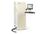
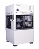
The wafer surface inspection system LS series can detect defects on unpatterned wafers with a mirror-finished surface. Applied technology of laser scattering achieves high sensitivity and high throughput detection of small contaminants and various types of defects on wafer surfaces prior to patterning. Wafer surface defects such as shallow scratch flatness defects, water marks, epi stacking faults, protrusions by the polishing process, and flatness defects caused during deposition cause problems in next-generation processes. The LS series achieve high sensitivity by detecting the light scattered from defects while suppressing background noise from the wafer surface. It is widely adopted to control contamination in the manufacturing of semiconductors on the 10-nm scale, and for delivery and incoming wafer quality control. For device manufacturer: incoming inspection and process tool monitoring use For tool and material manufacturer: process and material evaluation use For wafer supplier: outgoing inspection with wafer edge handling use
Description
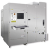
The wafer surface inspection system LS series can detect defects on unpatterned wafers with a mirror-finished surface. Applied technology of laser scattering achieves high sensitivity and high throughput detection of small contaminants and various types of defects on wafer surfaces prior to patterning. Wafer surface defects such as shallow scratch flatness defects, water marks, epi stacking faults, protrusions by the polishing process, and flatness defects caused during deposition cause problems in next-generation processes. The LS series achieve high sensitivity by detecting the light scattered from defects while suppressing background noise from the wafer surface. It is widely adopted to control contamination in the manufacturing of semiconductors on the 10-nm scale, and for delivery and incoming wafer quality control. For device manufacturer: incoming inspection and process tool monitoring use For tool and material manufacturer: process and material evaluation use For wafer supplier: outgoing inspection with wafer edge handling use

Suppliers

Company
Product
Description
Supplier Links
Wafer Surface Inspection System - LS Series - Hitachi High Technologies America, Inc.
Schaumburg, IL, USA
Wafer Surface Inspection System
LS Series
Wafer Surface Inspection System LS Series
The wafer surface inspection system LS series can detect defects on unpatterned wafers with a mirror-finished surface. Applied technology of laser scattering achieves high sensitivity and high throughput detection of small contaminants and various types of defects on wafer surfaces prior to patterning. Wafer surface defects such as shallow scratch flatness defects, water marks, epi stacking faults, protrusions by the polishing process, and flatness defects caused during deposition cause problems in next-generation processes. The LS series achieve high sensitivity by detecting the light scattered from defects while suppressing background noise from the wafer surface. It is widely adopted to control contamination in the manufacturing of semiconductors on the 10-nm scale, and for delivery and incoming wafer quality control. For device manufacturer: incoming inspection and process tool monitoring use For tool and material manufacturer: process and material evaluation use For wafer supplier: outgoing inspection with wafer edge handling use
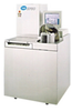
The wafer surface inspection system LS series can detect defects on unpatterned wafers with a mirror-finished surface. Applied technology of laser scattering achieves high sensitivity and high throughput detection of small contaminants and various types of defects on wafer surfaces prior to patterning. Wafer surface defects such as shallow scratch flatness defects, water marks, epi stacking faults, protrusions by the polishing process, and flatness defects caused during deposition cause problems in next-generation processes. The LS series achieve high sensitivity by detecting the light scattered from defects while suppressing background noise from the wafer surface. It is widely adopted to control contamination in the manufacturing of semiconductors on the 10-nm scale, and for delivery and incoming wafer quality control.

  • For device manufacturer: incoming inspection and process tool monitoring use
  • For tool and material manufacturer: process and material evaluation use
  • For wafer supplier: outgoing inspection with wafer edge handling use

Supplier's Site

Technical Specifications

  Hitachi High Technologies America, Inc.
Product Category Wafer and Thin Film Instrumentation
Product Number LS Series
Product Name Wafer Surface Inspection System
Form Factor ProbingSystem
Unlock Full Specs
to access all available technical data

Similar Products

Quasar200 - quasar200-and-pulsar600 - Cosmic Equipment SpA
Specs
Form Factor Monitor or instrument
Applications Wafer
View Details
EC-52000IC ION CLEANER -  - JEOL USA, Inc.
Specs
Form Factor Monitor or instrument
Mounting / Loading Floor
View Details
Arc discharge type high-vacuum ion plating system -  - Daitron Co., Ltd.
Specs
Applications CVD / PVD
View Details
Wafer Aligner -  - Palomar Technologies, Inc
Palomar Technologies, Inc
Specs
Form Factor Wafer Aligner
Mounting / Loading Benchtop
Technology Optical / Imaging
View Details