The 74HC594; 74HCT594 is an 8-bit serial-in/serial or parallel-out shift register with a storage register. Separate clock and reset inputs are provided on both shift and storage registers. The device features a serial input (DS) and a serial output (Q7S) to enable cascading. Data is shifted on the LOW-to-HIGH transitions of the SHCP input, and the data in the shift register is transferred to the storage register on a LOW-to-HIGH transition of the STCP input. If both clocks are connected together, the shift register will always be one clock pulse ahead of the storage register. A LOW level on one of the two register reset pins (SHR and STR) will clear the corresponding register. Inputs include clamp diodes. This enables the use of current limiting resistors to interface inputs to voltages in excess of VCC.
Features and benefits
Applications
Shift Shift Register 1 Element 8 Bit 16-SO
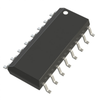
IC 8BIT SHIFT REGISTER 16-SOIC
IC 8BIT SHIFT REGISTER 16-SOIC
Shift Shift Register 1 Element 8 Bit 16-SO
| Nexperia B.V. | DigiKey | Lingto Electronic Limited | Shenzhen Shengyu Electronics Technology Limited | Quarktwin Technology Ltd. | |
|---|---|---|---|---|---|
| Product Category | Shift Registers | Shift Registers | Shift Registers | Shift Registers | Shift Registers |
| Product Number | 74HCT594D,112 | 1727-3456-ND | 74HCT594D,112 | 74HCT594D,112 | 74HCT594D,112 |
| Product Name | 8-bit shift register with output register | Shift Registers | Logic - Shift Registers | Integrated Circuits (ICs) - Logic - Shift Registers | Shift Registers |
| Supply Voltage | 5V; 4.5 - 5.5 | 4.5V ~ 5.5V | 4.5V ~ 5.5V | ||
| Features | ESD Protection | ||||
| Package Type | Other; SOT109-1 | SOIC; Other; "16-SOIC (0.154"", 3.90mm Width)" | SOIC | SOIC; Other; 16-SOIC (0.154\", 3.90mm Width) | |
| Logic Family | TTL | ||||
| Clock Frequency | 100 MHz |