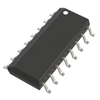
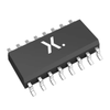
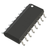
The 74HCT4538 is a dual retriggerable-rese
ttable monostable multivibrator. Each multivibrator has two trigger/retrigger inputs (nA and nB), a direct reset input (nCD), two complementary outputs (nQ and nQ), and two pins (nREXT/CEXT and nCEXT) for connecting the external timing components CEXT and REXT. Typical pulse width variation over temperature range is ± 0.2 %. The device may be triggered by either the positive or the negative edges of the input pulse. The duration and accuracy of the output pulse are determined by the external timing components CEXT and REXT. The output pulse width (TW) is equal to 0.7 × REXT × CEXT. The linear design techniques guarantee precise control of the output pulse width. A LOW level at nCD terminates the output pulse immediately. Schmitt-trigger action in the trigger inputs makes the circuit highly tolerant to slower rise and fall times. Inputs include clamp diodes. This enables the use of current limiting resistors to interface inputs to voltages in excess of VCC.
Features and benefits
Tolerant of slow trigger rise and fall times
High noise immunity
Separate reset inputs
Triggering from falling or rising edge
Complies with JEDEC standard no. 7A
Wide supply voltage range from 4.5 to 5.5 V
CMOS low power dissipation
TTL input levels
Latch-up performance exceeds 100 mA per JESD 78 Class II Level B
ESD protection:
HBM: ANSI/ESDA/JEDEC JS-001 class 2 exceeds 2000 V
CDM: ANSI/ESDA/JEDEC JS-002 class C3 exceeds 1000 V
Specified from -40 °C to +85 °C and from -40 °C to +125 °C
The 74HCT4538 is a dual retriggerable-resettable monostable multivibrator. Each multivibrator has two trigger/retrigger inputs (nA and nB), a direct reset input (nCD), two complementary outputs (nQ and nQ), and two pins (nREXT/CEXT and nCEXT) for connecting the external timing components CEXT and REXT. Typical pulse width variation over temperature range is ± 0.2 %. The device may be triggered by either the positive or the negative edges of the input pulse. The duration and accuracy of the output pulse are determined by the external timing components CEXT and REXT. The output pulse width (TW) is equal to 0.7 × REXT × CEXT. The linear design techniques guarantee precise control of the output pulse width. A LOW level at nCD terminates the output pulse immediately. Schmitt-trigger action in the trigger inputs makes the circuit highly tolerant to slower rise and fall times. Inputs include clamp diodes. This enables the use of current limiting resistors to interface inputs to voltages in excess of VCC.
Features and benefits
- Tolerant of slow trigger rise and fall times
- High noise immunity
- Separate reset inputs
- Triggering from falling or rising edge
- Complies with JEDEC standard no. 7A
- Wide supply voltage range from 4.5 to 5.5 V
- CMOS low power dissipation
- TTL input levels
- Latch-up performance exceeds 100 mA per JESD 78 Class II Level B
- ESD protection:
- HBM: ANSI/ESDA/JEDEC JS-001 class 2 exceeds 2000 V
- CDM: ANSI/ESDA/JEDEC JS-002 class C3 exceeds 1000 V
- Specified from -40 °C to +85 °C and from -40 °C to +125 °C
