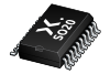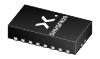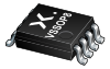
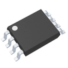
Nexperia B.V. Low-power dual D-type flip-flop; positive-edge trigger 74AUP2G79DC,125

Description
The 74AUP2G79 provides the dual positive-edge triggered D-type flip-flop. Information on the data input (nD) is transferred to the nQ output on the LOW-to-HIGH transition of the clock pulse (nCP). The nD input must be stable one set-up time prior to the LOW-to-HIGH clock transition for predictable operation. Schmitt trigger action at all inputs makes the circuit tolerant to slower input rise and fall times across the entire VCC range from 0.8 V to 3.6 V. This device ensures a very low static and dynamic power consumption across the entire VCC range from 0.8 V to 3.6 V. This device is fully specified for partial power-down applications using IOFF. The IOFF circuitry disables the output, preventing a damaging backflow current through the device when it is powered down. Features and benefits Wide supply voltage range from 0.8 V to 3.6 V High noise immunity Complies with JEDEC standards: JESD8-12 (0.8 V to 1.3 V) JESD8-11 (0.9 V to 1.65 V) JESD8-7 (1.2 V to 1.95 V) JESD8-5 (1.8 V to 2.7 V) JESD8-B (2.7 V to 3.6 V) Low static power consumption; ICC = 0.9 μA (maximum) Latch-up performance exceeds 100 mA per JESD78 Class II Inputs accept voltages up to 3.6 V Low noise overshoot and undershoot < 10 % of VCC IOFF circuitry provides partial Power-down mode operation ESD protection: HBM: ANSI/ESDA/JEDEC JS-001 class 3A exceeds 5000 V CDM: ANSI/ESDA/JEDEC JS-002 class C3 exceeds 1000 V Multiple package options Specified from -40 °C to +85 °C and -40 °C to +125 °C
Request a Quote Datasheet
Description
The 74AUP2G79 provides the dual positive-edge triggered D-type flip-flop. Information on the data input (nD) is transferred to the nQ output on the LOW-to-HIGH transition of the clock pulse (nCP). The nD input must be stable one set-up time prior to the LOW-to-HIGH clock transition for predictable operation. Schmitt trigger action at all inputs makes the circuit tolerant to slower input rise and fall times across the entire VCC range from 0.8 V to 3.6 V. This device ensures a very low static and dynamic power consumption across the entire VCC range from 0.8 V to 3.6 V. This device is fully specified for partial power-down applications using IOFF. The IOFF circuitry disables the output, preventing a damaging backflow current through the device when it is powered down. Features and benefits Wide supply voltage range from 0.8 V to 3.6 V High noise immunity Complies with JEDEC standards: JESD8-12 (0.8 V to 1.3 V) JESD8-11 (0.9 V to 1.65 V) JESD8-7 (1.2 V to 1.95 V) JESD8-5 (1.8 V to 2.7 V) JESD8-B (2.7 V to 3.6 V) Low static power consumption; ICC = 0.9 μA (maximum) Latch-up performance exceeds 100 mA per JESD78 Class II Inputs accept voltages up to 3.6 V Low noise overshoot and undershoot < 10 % of VCC IOFF circuitry provides partial Power-down mode operation ESD protection: HBM: ANSI/ESDA/JEDEC JS-001 class 3A exceeds 5000 V CDM: ANSI/ESDA/JEDEC JS-002 class C3 exceeds 1000 V Multiple package options Specified from -40 °C to +85 °C and -40 °C to +125 °C
Request a Quote Datasheet

Suppliers

Company
Product
Description
Supplier Links
Low-power dual D-type flip-flop; positive-edge trigger - 74AUP2G79DC,125 - Nexperia B.V.
Nijmegen, Netherlands
Low-power dual D-type flip-flop; positive-edge trigger
74AUP2G79DC,125
Low-power dual D-type flip-flop; positive-edge trigger 74AUP2G79DC,125
The 74AUP2G79 provides the dual positive-edge triggered D-type flip-flop. Information on the data input (nD) is transferred to the nQ output on the LOW-to-HIGH transition of the clock pulse (nCP). The nD input must be stable one set-up time prior to the LOW-to-HIGH clock transition for predictable operation. Schmitt trigger action at all inputs makes the circuit tolerant to slower input rise and fall times across the entire VCC range from 0.8 V to 3.6 V. This device ensures a very low static and dynamic power consumption across the entire VCC range from 0.8 V to 3.6 V. This device is fully specified for partial power-down applications using IOFF. The IOFF circuitry disables the output, preventing a damaging backflow current through the device when it is powered down. Features and benefits Wide supply voltage range from 0.8 V to 3.6 V High noise immunity Complies with JEDEC standards: JESD8-12 (0.8 V to 1.3 V) JESD8-11 (0.9 V to 1.65 V) JESD8-7 (1.2 V to 1.95 V) JESD8-5 (1.8 V to 2.7 V) JESD8-B (2.7 V to 3.6 V) Low static power consumption; ICC = 0.9 μA (maximum) Latch-up performance exceeds 100 mA per JESD78 Class II Inputs accept voltages up to 3.6 V Low noise overshoot and undershoot < 10 % of VCC IOFF circuitry provides partial Power-down mode operation ESD protection: HBM: ANSI/ESDA/JEDEC JS-001 class 3A exceeds 5000 V CDM: ANSI/ESDA/JEDEC JS-002 class C3 exceeds 1000 V Multiple package options Specified from -40 °C to +85 °C and -40 °C to +125 °C

The 74AUP2G79 provides the dual positive-edge triggered D-type flip-flop. Information on the data input (nD) is transferred to the nQ output on the LOW-to-HIGH transition of the clock pulse (nCP). The nD input must be stable one set-up time prior to the LOW-to-HIGH clock transition for predictable operation.

Schmitt trigger action at all inputs makes the circuit tolerant to slower input rise and fall times across the entire VCC range from 0.8 V to 3.6 V.

This device ensures a very low static and dynamic power consumption across the entire VCC range from 0.8 V to 3.6 V.

This device is fully specified for partial power-down applications using IOFF. The IOFF circuitry disables the output, preventing a damaging backflow current through the device when it is powered down.

Features and benefits

  • Wide supply voltage range from 0.8 V to 3.6 V
  • High noise immunity
  • Complies with JEDEC standards:
    • JESD8-12 (0.8 V to 1.3 V)
    • JESD8-11 (0.9 V to 1.65 V)
    • JESD8-7 (1.2 V to 1.95 V)
    • JESD8-5 (1.8 V to 2.7 V)
    • JESD8-B (2.7 V to 3.6 V)
  • Low static power consumption; ICC = 0.9 μA (maximum)
  • Latch-up performance exceeds 100 mA per JESD78 Class II
  • Inputs accept voltages up to 3.6 V
  • Low noise overshoot and undershoot < 10 % of VCC
  • IOFF circuitry provides partial Power-down mode operation
  • ESD protection:
    • HBM: ANSI/ESDA/JEDEC JS-001 class 3A exceeds 5000 V
    • CDM: ANSI/ESDA/JEDEC JS-002 class C3 exceeds 1000 V
  • Multiple package options
  • Specified from -40 °C to +85 °C and -40 °C to +125 °C
Supplier's Site Datasheet
Flip Flops - 1727-6885-6-ND - DigiKey
Thief River Falls, MN, United States
Flip Flops
1727-6885-6-ND
Flip Flops 1727-6885-6-ND
"Flip Flop 2 Element D-Type 1 Bit Positive Edge 8-VFSOP (0.091"", 2.30mm Width)"

"Flip Flop 2 Element D-Type 1 Bit Positive Edge 8-VFSOP (0.091"", 2.30mm Width)"

Buy Now Datasheet
Flip Flops - 1727-6885-1-ND - DigiKey
Thief River Falls, MN, United States
Flip Flops
1727-6885-1-ND
Flip Flops 1727-6885-1-ND
"Flip Flop 2 Element D-Type 1 Bit Positive Edge 8-VFSOP (0.091"", 2.30mm Width)"

"Flip Flop 2 Element D-Type 1 Bit Positive Edge 8-VFSOP (0.091"", 2.30mm Width)"

Buy Now Datasheet
Flip Flops - 1727-6885-2-ND - DigiKey
Thief River Falls, MN, United States
Flip Flops
1727-6885-2-ND
Flip Flops 1727-6885-2-ND
"Flip Flop 2 Element D-Type 1 Bit Positive Edge 8-VFSOP (0.091"", 2.30mm Width)"

"Flip Flop 2 Element D-Type 1 Bit Positive Edge 8-VFSOP (0.091"", 2.30mm Width)"

Buy Now Datasheet
Flip Flops - 74AUP2G79DC,125 - Quarktwin Technology Ltd.
Shenzhen, Guangdong, China
Flip Flop 2 Element D-Type 1 Bit Positive Edge 8-VFSOP (0.091", 2.30mm Width)

Flip Flop 2 Element D-Type 1 Bit Positive Edge 8-VFSOP (0.091", 2.30mm Width)

Buy Now Datasheet
Logic - Flip Flops - 74AUP2G79DC,125 - Lingto Electronic Limited
Shenzhen, China
Logic - Flip Flops
74AUP2G79DC,125
Logic - Flip Flops 74AUP2G79DC,125
IC FF D-TYPE DUAL 1BIT 8VSSOP

IC FF D-TYPE DUAL 1BIT 8VSSOP

Supplier's Site Datasheet

Technical Specifications

  Nexperia B.V. DigiKey Quarktwin Technology Ltd. Lingto Electronic Limited
Product Category Flip-Flops Flip-Flops Flip-Flops Flip-Flops
Product Number 74AUP2G79DC,125 1727-6885-6-ND 74AUP2G79DC,125 74AUP2G79DC,125
Product Name Low-power dual D-type flip-flop; positive-edge trigger Flip Flops Flip Flops Logic - Flip Flops
Flip-Flop Type D D D
Triggering Positive-edge Triggered Positive-edge Triggered
Supply Voltage +4.6 0.8V ~ 3.6V 3.6V; 0.8V ~ 3.6V
Features ESD Protection
Operating Temperature 125 C (257 F) -40 to 125 C (-40 to 257 F) -40 to 125 C (-40 to 257 F)
Unlock Full Specs
to access all available technical data

Similar Products

Flip Flops - 1727-2447-ND - DigiKey
Specs
Flip-Flop Type D
Triggering Positive-edge Triggered
Supply Voltage 2.3V ~ 2.7V, 3V ~ 3.6V
View Details
4 suppliers
Dual D-type flip-flop with set and reset; positive-edge trigger - 74AHC74BQ-Q100X - Nexperia B.V.
Specs
Flip-Flop Type D
Triggering Positive-edge Triggered
Supply Voltage +7.0
View Details
6 suppliers
Octal D-type flip-flop; positive edge-trigger; 3-state - 74AHCT374PW-Q100J - Nexperia B.V.
Specs
Flip-Flop Type D
Triggering Positive-edge Triggered
Supply Voltage +7.0
View Details
5 suppliers
Octal D-type flip-flop with data enable; positive-edge trigger - 74HC377D-Q100J - Nexperia B.V.
Specs
Flip-Flop Type D
Triggering Positive-edge Triggered
Supply Voltage +7
View Details
5 suppliers