
Description
What is 2 Layer Aluminum PCB (Double-Sided Alu PCB)
The 2 Layer Aluminum substrate is normally more complicated, and it consists of five structures: Layer, dielectric Layer, Aluminum base Layer, dielectric layer and the circuit layer.
The Aluminum material of the Aluminum base PCB layer has high thermal conductivity and is suitable for aluminum alloy plates with conventional processing methods such as drilling, punching, and copper.
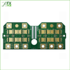
2 Layer Aluminum PCB is called double-sided Aluminum PCB. its substrates can still only have one LED, a single layer trace, double-sided Aluminum substrates can be used for LEDs on both sides, and double-sided Aluminum substrates require two layers of trace, then single-sided Aluminum substrated and double-sided Aluminum substrate processing.
Compared with the single-sided Aluminum PCB, the double-sided Alu board has more stamping process and electroplating processes, but the price is higher. As the 2 Layer Aluminum manufacturing process is more difficult, you need to drill holes twice (as it is not easy to plate copper on the Aluminum base material directly)
2 Layer Aluminum PCB Stack up
2 Layer / Double-Sided Aluminum Base Board PCB Capability:
Items Capability
Board Classification Aluminum Base, Copper Base, Ceramics Base, Copper-Clad, Combined Bade Board
Material Domestic Aluminum, Domestic copper,lmported aluminum, lmported copper
Surface Treatment HASL/ENIG/OSP/Silver
Layer Count Single-sided printed board/Double-sided printed board
Max.Board Size 1200mm*480mm
Min. Board Size 5mm*5mm
Trace width/Space 0.1mm/0.1mm
Warp and twist <=0.5%(Thickness:1.6
Board Thickness 0.5mm-5.0mm
Copper Thickness 35um/70um/105um/140u
Min. punching Hole 1.0mm(Board thickness below1.0mm)
Min Hole Diameter 0.6mm
Min. Solder Mask Opening 0.35mm
DELIVERY TIME:
Single Sided aluminum based board Double-sided aluminum-based board Single sided copper based board Double sided copper based board Ceramic based board
Prototype 5 Working Days 14 Working Days 9 Working Days 16 Working Days 8 Working Days
Mass Production 8 Working Days 17 Working Days 12 Working Days 19 Working Days 11 Working Days
MP in repeat order 7 Working Days 16 Working Days 11 Working Days 18 Working Days 10 Working Days
MAJOR SUPPLIER:
Supplier Material Origin
Boyu Aluminum Huizhou China
Mingrong Aluminum Shenzhen China
Naya Metal Copper Dongguan China
Shengyi Copper Clad Laminate Guangdong China
Taiyo Solder Mask Japan
Guangxin Solder Mask Guangzhou China
PROCESS-FlOW:
As an Aluminum base PCB factory, FX PCB will be glad to quote you the price for your 2 Layer /double-sided Aluminum PCB, please send us your inquiry to info@sfxpcb.com
| FX PCB Co., Ltd. | |
|---|---|
| Product Category | Printed Circuit Substrate Materials (PCB / PWB) |
| Product Name | 2 Layer / Double Sided Aluminum PCB |
| Materials | Aluminum Foil; Copper Foil; Domestic Aluminum, Domestic copper,lmported aluminum, lmported copper |