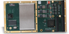
XMC730 mezzanine modules provide a variety of I/O functions on a single plug-in card. These new high-density modules perform both high-speed and high resolution A/D and D/A conversion and also handle digital I/O and counter/timer functions.
• Analog input • Analog output • Digital I/O • Counter/timers • Conduction-cooled options
Performance Specifications
■ Analog Input
Input channels: 16 differential, voltage (non-isolated).
Resolution: 16 bits.
Conversion rate: 791,139.24Hz maximum.
Settling time: Full-scale step 420 ns to 0.005% of FSR.
Input ranges: - Software-selectable on a per channel basis. - Bipolar: ±10.24V, ±10.0V ±5.12V, ±5.0V. - Unipolar: 0 to 10.24V, 0 to 10.0V, 0 to 5.12V.
Calibrated error: ±3.125 LSB max. (0 to 5.12V). ±2.125 LSB max. (all other ranges).
■ Analog Output
Output channels: 8 single-ended voltage (non-isolated).
Resolution: 16 bits.
Settling Time: 12.5 µs 20 V step to 1 LSB maximum. 8.5 µs 10 V step to 1 LSB maximum. 7.5 µs typical.
Output ranges (software-selectable
): - Bipolar: ±10V, ±5V, ±3V, -2.5 to +7.5V. - Unipolar: 0 to 10V, 0 to 5V.
Output current: ± 10mA maximum (minimum load resistance of 1KΩ with a 10V output).
Calibrated error: ±2.125 LSB (±0.0032% FSR) max.
■ Digital I/O
Input/output range: 0 to 5V.
Signal thresholds: VIH: 2.0V minimum. VIL: 0.8V maximum. IOH: ─24 mA maximum. IOL: 24mA maximum. VOH: 3.7V minimum VCCA. VOL: 0.55V maximum VCCA.
Minimum pulse: 32nS.
Debounce: Filters signals with duration <2.4 µs.
■ Counter/Timer
Configuration: 32-bit timer. Counter input: TTL input port. Counter output: MOSFET output port. Counter output pull-up voltage: +5V or 12V with 1K pull-up, set by DIP switch. Internal clock: 62.5MHz, 15.625MHz, 7.8125MHz, 3.90625MHz, 1.953125MHz.
■ XMC Compliance
Complies with ANSI/VITA 42.0 specification for XMC module mechanicals and connectors. Complies with ANSI/VITA 42.3 specification for XMC modules with PCI Express interface. Electrical/mechanica
l interface: Single-Width Module.
■ PCIE Compliance
Conforms to PCI Express Base Specification, Revision 2.1. Gen1 PCIe interface. BAR0 memory size: 1M Byte.
■ Environmental
Operating temperature: XMC730: 0 to 70°C (200 LFM airflow). XMC730E: -40 to 85°C (200 LFM airflow). XMC730CC: -40 to 85°C (cold plate).
Storage temperature: -55 to 100°C.
Relative humidity: 5 to 95% non-condensing.
Shock, operating: Designed to comply with VITA 47 Class OS1.
Vibration, random operating: Designed to comply with VITA 47 Class V1.
Power: 3.3V ±5%: 0.567A typical, 0.7A maximum. VPWR ±5%: 0.10A typical, 0.11A maximum. +12V ±5%: 0.03A typical, 0.0374 maximum.
Features & Benefits
Analog Inputs
• 16 differential (±10.24V, ±10.0V, ±5.12V, ±5.0V, 0 to 10.24V, 0 to 10.0V, 0 to 5.12V ranges) • 16-bit ADC with integral sample-and-hold and reference • 1.264μS conversion time (791KHz rate) • 1026 sample FIFO buffer • Programmable FIFO threshold conditions for interrupts, DMA transfers, and flags • User-programmable channel conversion sequence and timing • External trigger input or output • Factory calibration constants stored in on-board flash memory for error correction
Analog Outputs
• Eight analog output channels (±3V, ±5V, ±10V, -2.5 to +7.5V, 0-5V, and 0-10V ranges) • Individual 16-bit DACs per channel with 7.5μS settling time • Flexible operating mode, trigger, and memory allocation • Configurable for direct access, single burst, continuous, or streaming (FIFO) output • Reliable software calibration with coefficients stored on-board • FIFO for waveform generation • Interrupt on user-programmable FIFO threshold • Shared 64K x 16-bit sample memory
Digital I/O
• 16 bidirectional input/output channels (direction configured in 8-channel groups) • TTL-compatible thresholds • Programmable change-of-state/leve
l interrupts • Failsafe power-up and system reset
Counter/Timers
• Multi-function 32-bit counter/timer – Quadrature Position measurement – Pulse Width modulation – Watchdog timer – Event counter – Frequency measurement – Pulse-width or period measurement
• One-shot and repetitive one-shot pulse waveform generation • Programmable interface polarity • Internal or external triggering • CMOS compatible thresholds
General
• DMA transfer support to move data between module memory and PCIe bus • Software development tools for VxWorks®, Linux®, and Windows® environments
XMC730 mezzanine modules provide a variety of I/O functions on a single plug-in card. These new high-density modules perform both high-speed and high resolution A/D and D/A conversion and also handle digital I/O and counter/timer functions.
• Analog input
• Analog output
• Digital I/O
• Counter/timers
• Conduction-cooled options
Performance Specifications
■ Analog Input
Input channels: 16 differential, voltage (non-isolated).
Resolution: 16 bits.
Conversion rate: 791,139.24Hz maximum.
Settling time: Full-scale step 420 ns to 0.005% of FSR.
Input ranges:
- Software-selectable on a per channel basis.
- Bipolar: ±10.24V, ±10.0V ±5.12V, ±5.0V.
- Unipolar: 0 to 10.24V, 0 to 10.0V, 0 to 5.12V.
Calibrated error:
±3.125 LSB max. (0 to 5.12V).
±2.125 LSB max. (all other ranges).
■ Analog Output
Output channels: 8 single-ended voltage (non-isolated).
Resolution: 16 bits.
Settling Time:
12.5 µs 20 V step to 1 LSB maximum.
8.5 µs 10 V step to 1 LSB maximum.
7.5 µs typical.
Output ranges (software-selectable):
- Bipolar: ±10V, ±5V, ±3V, -2.5 to +7.5V.
- Unipolar: 0 to 10V, 0 to 5V.
Output current: ± 10mA maximum (minimum load resistance of 1KΩ with a 10V output).
Calibrated error: ±2.125 LSB (±0.0032% FSR) max.
■ Digital I/O
Input/output range: 0 to 5V.
Signal thresholds:
VIH: 2.0V minimum.
VIL: 0.8V maximum.
IOH: ─24 mA maximum.
IOL: 24mA maximum.
VOH: 3.7V minimum VCCA.
VOL: 0.55V maximum VCCA.
Minimum pulse: 32nS.
Debounce: Filters signals with duration <2.4 µs.
■ Counter/Timer
Configuration: 32-bit timer.
Counter input: TTL input port.
Counter output: MOSFET output port.
Counter output pull-up voltage: +5V or 12V with 1K pull-up, set by DIP switch.
Internal clock: 62.5MHz, 15.625MHz, 7.8125MHz, 3.90625MHz, 1.953125MHz.
■ XMC Compliance
Complies with ANSI/VITA 42.0 specification for XMC module mechanicals and connectors.
Complies with ANSI/VITA 42.3 specification for XMC modules with PCI Express interface.
Electrical/mechanical interface: Single-Width Module.
■ PCIE Compliance
Conforms to PCI Express Base Specification, Revision 2.1.
Gen1 PCIe interface.
BAR0 memory size: 1M Byte.
■ Environmental
Operating temperature:
XMC730: 0 to 70°C (200 LFM airflow).
XMC730E: -40 to 85°C (200 LFM airflow).
XMC730CC: -40 to 85°C (cold plate).
Storage temperature: -55 to 100°C.
Relative humidity: 5 to 95% non-condensing.
Shock, operating: Designed to comply with VITA 47 Class OS1.
Vibration, random operating: Designed to comply with VITA 47 Class V1.
Power:
3.3V ±5%: 0.567A typical, 0.7A maximum.
VPWR ±5%: 0.10A typical, 0.11A maximum.
+12V ±5%: 0.03A typical, 0.0374 maximum.
Features & Benefits
Analog Inputs
• 16 differential (±10.24V, ±10.0V, ±5.12V, ±5.0V, 0 to 10.24V, 0 to 10.0V, 0 to 5.12V ranges)
• 16-bit ADC with integral sample-and-hold and reference
• 1.264μS conversion time (791KHz rate)
• 1026 sample FIFO buffer
• Programmable FIFO threshold conditions for interrupts, DMA transfers, and flags
• User-programmable channel conversion sequence and timing
• External trigger input or output
• Factory calibration constants stored in on-board flash memory for error correction
Analog Outputs
• Eight analog output channels (±3V, ±5V, ±10V, -2.5 to +7.5V, 0-5V, and 0-10V ranges)
• Individual 16-bit DACs per channel with 7.5μS settling time
• Flexible operating mode, trigger, and memory allocation
• Configurable for direct access, single burst, continuous, or streaming (FIFO) output
• Reliable software calibration with coefficients stored on-board
• FIFO for waveform generation
• Interrupt on user-programmable FIFO threshold
• Shared 64K x 16-bit sample memory
Digital I/O
• 16 bidirectional input/output channels (direction configured in 8-channel groups)
• TTL-compatible thresholds
• Programmable change-of-state/level interrupts
• Failsafe power-up and system reset
Counter/Timers
• Multi-function 32-bit counter/timer
– Quadrature Position measurement
– Pulse Width modulation
– Watchdog timer
– Event counter
– Frequency measurement
– Pulse-width or period measurement
• One-shot and repetitive one-shot pulse waveform generation
• Programmable interface polarity
• Internal or external triggering
• CMOS compatible thresholds
General
• DMA transfer support to move data between module memory and PCIe bus
• Software development tools for VxWorks®, Linux®, and Windows® environments