Nexperia B.V. 8-bit serial-in, serial or parallel-out shift register with output latches; 3-state 74HCT595D-Q100,118

Request a Quote Datasheet

Suppliers

Company
Product
Description
Supplier Links
8-bit serial-in, serial or parallel-out shift register with output latches; 3-state - 74HCT595D-Q100,118 - Nexperia B.V.
Nijmegen, Netherlands
8-bit serial-in, serial or parallel-out shift register with output latches; 3-state
74HCT595D-Q100,118
8-bit serial-in, serial or parallel-out shift register with output latches; 3-state 74HCT595D-Q100,118
The 74HC595-Q100; 74HCT595-Q100 is an 8-bit serial-in/serial or parallel-out shift register with a storage register and 3-state outputs. Both the shift and storage register have separate clocks. The device features a serial input (DS) and a serial output (Q7S) to enable cascading and an asynchronous reset MR input. A LOW on MR will reset the shift register. Data is shifted on the LOW-to-HIGH transitions of the SHCP input. The data in the shift register is transferred to the storage register on a LOW-to-HIGH transition of the STCP input. If both clocks are connected together, the shift register will always be one clock pulse ahead of the storage register. Data in the storage register appears at the output whenever the output enable input (OE) is LOW. A HIGH on OE causes the outputs to assume a high-impedance OFF-state. Operation of the OE input does not affect the state of the registers. Inputs include clamp diodes. This enables the use of current limiting resistors to interface inputs to voltages in excess of VCC. This product has been qualified to the Automotive Electronics Council (AEC) standard Q100 (Grade 1) and is suitable for use in automotive applications. Features and benefits Automotive product qualification in accordance with AEC-Q100 (Grade 1) Specified from -40 °C to +85 °C and from -40 °C to +125 °C 8-bit serial input 8-bit serial or parallel output Storage register with 3-state outputs Shift register with direct clear 100 MHz (typical) shift out frequency Complies with JEDEC standard no. 7A Input levels: For 74HC595-Q100: CMOS level For 74HCT595-Q100: TTL level ESD protection: HBM: ANSI/ESDA/JEDEC JS-001 class 2 exceeds 2000 V CDM: ANSI/ESDA/JEDEC JS-002 class C3 exceeds 1000 V Multiple package options DHVQFN package with Side-Wettable Flanks enabling Automatic Optical Inspection (AOI) of solder joints Applications Serial-to-parallel data conversion Remote control holding register

The 74HC595-Q100; 74HCT595-Q100 is an 8-bit serial-in/serial or parallel-out shift register with a storage register and 3-state outputs. Both the shift and storage register have separate clocks. The device features a serial input (DS) and a serial output (Q7S) to enable cascading and an asynchronous reset MR input. A LOW on MR will reset the shift register. Data is shifted on the LOW-to-HIGH transitions of the SHCP input. The data in the shift register is transferred to the storage register on a LOW-to-HIGH transition of the STCP input. If both clocks are connected together, the shift register will always be one clock pulse ahead of the storage register. Data in the storage register appears at the output whenever the output enable input (OE) is LOW. A HIGH on OE causes the outputs to assume a high-impedance OFF-state. Operation of the OE input does not affect the state of the registers. Inputs include clamp diodes. This enables the use of current limiting resistors to interface inputs to voltages in excess of VCC.

This product has been qualified to the Automotive Electronics Council (AEC) standard Q100 (Grade 1) and is suitable for use in automotive applications.

Features and benefits

  • Automotive product qualification in accordance with AEC-Q100 (Grade 1)
    • Specified from -40 °C to +85 °C and from -40 °C to +125 °C
  • 8-bit serial input
  • 8-bit serial or parallel output
  • Storage register with 3-state outputs
  • Shift register with direct clear
  • 100 MHz (typical) shift out frequency
  • Complies with JEDEC standard no. 7A
  • Input levels:
    • For 74HC595-Q100: CMOS level
    • For 74HCT595-Q100: TTL level
  • ESD protection:
    • HBM: ANSI/ESDA/JEDEC JS-001 class 2 exceeds 2000 V
    • CDM: ANSI/ESDA/JEDEC JS-002 class C3 exceeds 1000 V
  • Multiple package options
  • DHVQFN package with Side-Wettable Flanks enabling Automatic Optical Inspection (AOI) of solder joints

Applications

  • Serial-to-parallel data conversion
  • Remote control holding register
Supplier's Site Datasheet
Integrated Circuits (ICs) - Logic - Shift Registers - 74HCT595D-Q100,118 - Shenzhen Shengyu Electronics Technology Limited
Futian, China
Integrated Circuits (ICs) - Logic - Shift Registers
74HCT595D-Q100,118
Integrated Circuits (ICs) - Logic - Shift Registers 74HCT595D-Q100,118
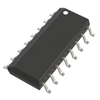
IC SHIFT REGISTER 8BIT 16SOIC

IC SHIFT REGISTER 8BIT 16SOIC
Supplier's Site
Logic - Shift Registers - 74HCT595D-Q100,118 - Lingto Electronic Limited
Shenzhen, China
Logic - Shift Registers
74HCT595D-Q100,118
Logic - Shift Registers 74HCT595D-Q100,118
IC SHIFT REGISTER 8BIT 16SOIC

IC SHIFT REGISTER 8BIT 16SOIC

Supplier's Site Datasheet
Shift Registers - 1727-8014-2-ND - DigiKey
Thief River Falls, MN, United States
Shift Registers
1727-8014-2-ND
Shift Registers 1727-8014-2-ND
Shift Shift Register 1 Element 8 Bit 16-SO

Shift Shift Register 1 Element 8 Bit 16-SO

Supplier's Site Datasheet
Shift Registers - 1727-8014-1-ND - DigiKey
Thief River Falls, MN, United States
Shift Registers
1727-8014-1-ND
Shift Registers 1727-8014-1-ND
Shift Shift Register 1 Element 8 Bit 16-SO
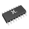
Shift Shift Register 1 Element 8 Bit 16-SO

Supplier's Site Datasheet
Shift Registers - 1727-8014-6-ND - DigiKey
Thief River Falls, MN, United States
Shift Registers
1727-8014-6-ND
Shift Registers 1727-8014-6-ND
Shift Shift Register 1 Element 8 Bit 16-SO

Shift Shift Register 1 Element 8 Bit 16-SO

Supplier's Site Datasheet
Shift Registers - 74HCT595D-Q100,118 - Quarktwin Technology Ltd.
Shenzhen, Guangdong, China
Shift Registers
74HCT595D-Q100,118
Shift Registers 74HCT595D-Q100,118
Shift Shift Register 1 Element 8 Bit 16-SO

Shift Shift Register 1 Element 8 Bit 16-SO

Supplier's Site Datasheet

Technical Specifications

  Nexperia B.V. Shenzhen Shengyu Electronics Technology Limited Lingto Electronic Limited DigiKey Quarktwin Technology Ltd.
Product Category Shift Registers Shift Registers Shift Registers Shift Registers Shift Registers
Product Number 74HCT595D-Q100,118 74HCT595D-Q100,118 74HCT595D-Q100,118 1727-8014-2-ND 74HCT595D-Q100,118
Product Name 8-bit serial-in, serial or parallel-out shift register with output latches; 3-state Integrated Circuits (ICs) - Logic - Shift Registers Logic - Shift Registers Shift Registers Shift Registers
Supply Voltage 5V; 4.5 - 5.5 4.5V ~ 5.5V 4.5V ~ 5.5V
Features ESD Protection
Package Type Other; SOT109-1 SOIC SOIC; Other; 16-SOIC (0.154", 3.90mm Width) SOIC; Other; 16-SOIC (0.154\", 3.90mm Width)
Logic Family TTL
Clock Frequency 57 MHz
Unlock Full Specs
to access all available technical data

Similar Products

8-bit serial-in, parallel-out shift register - 74HC164D-Q100J - Nexperia B.V.
Specs
Register Type Serial In / Parallel Out
Supply Voltage 2.5V; 3V; 3.3V; 3.6V; 5V; 2.0 - 6.0
Features ESD Protection
View Details
7 suppliers
8-bit shift register with output register - 74HC594BQ-Q100X - Nexperia B.V.
Specs
Supply Voltage 2.5V; 3V; 3.3V; 3.6V; 5V; 2.0 - 6.0
Features ESD Protection
Package Type Other; SOT763-1
View Details
3 suppliers
8-bit serial-in, parallel-out shift register - 74HC164BQ-Q100X - Nexperia B.V.
Specs
Register Type Serial In / Parallel Out
Supply Voltage 2.5V; 3V; 3.3V; 3.6V; 5V; 2.0 - 6.0
Features ESD Protection
View Details
7 suppliers
Dual supply 8-bit serial-in/serial-out or parallel-out shift register; 3-state - 74LVC8T595BQX - Nexperia B.V.
Specs
Register Type Serial In / Serial Out - Shift Right; Serial In / Parallel Out
Supply Voltage 1.1 - 5.5
Output Characteristics 3-State
View Details
6 suppliers