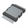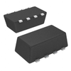

The Si5511DC-T1-GE3 is a twin N- and P-channel MOSFET array in a 1206-8 ChipFET package, designed for use in portable devices and buck-boost circuits. It is lead-free and halogen-free, compliant with RoHS Directive 2002/95/EC and IEC 61249-2-21. The devices feature a 30 V drain-source voltage rating, with continuous drain currents of 4 A (N-channel) and -3.6 A (P-channel) at 25°C case temperature, reduced to 3.9 A and -1.8 A at 70°C ambient. Maximum power dissipation is 1.33 W (N-channel) and 0.84 W (P-channel) at 70°C ambient. On-state resistance is 0.055 Ω at 4.5 V gate bias (N-channel) and 0.150 Ω at -4.5 V gate bias (P-channel). Total gate charge is 7.1 nC (N-channel) and 6.2 nC (P-channel) under specified conditions. Operating junction and storage temperature range is -55°C to 150°C. Thermal resistance is 50 °C/W (N-channel) and 77 °C/W (P-channel) junction-to-ambient.
Win Source Part Number: 1278481-SI5511DC-T1-
Category: Discrete Semiconductor Products>Transistors
Series: TrenchFET®
Package: Tape & Reel
Standard Package: 3,000
Mounting: SMD (SMT)
FET Type: N and P-Channel
FET Feature: Logic Level Gate
Drain to Source Voltage (Vdss): 30V
Current - Continuous Drain (Id) @ 25°C: 4A, 3.6A
Rds On (Max) @ Id, Vgs: 55mOhm @ 4.8A, 4.5V
Vgs(th) (Max) @ Id: 2V @ 250µA
Power - Max: 3.1W, 2.6W
Package / Case: 8-SMD, Flat Lead
Supplier Device Package: 1206-8 ChipFET™
Gate Charge (Qg) (Max) @ Vgs: 7.1nC @ 5V
Input Capacitance (Ciss) (Max) @ Vds: 435pF @ 15V
Temperature Range - Operating: -55°C ~ 150°C (TJ)
ECCN: EAR99
Fake Threat In the Open Market: 76 pct.
MSL Level: 1 (Unlimited)
REACH Status: REACH Unaffected
HTSUS: 8541.29.0095
Mfr: Vishay Siliconix
Other Names: SI5511DC-T1-GE3CT,SI
Base Product Number: SI5511
Product Status: Obsolete
| Win Source Electronics | |
|---|---|
| Product Category | Transistors |
| Product Number | 1278481-SI5511DC-T1-GE3 |
| Product Name | Discrete Semiconductor Products - Transistors - FETs, MOSFETs - Arrays |
| Polarity | P-Channel |