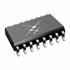
The SN74LVC125ANS is a quadruple bus buffer gate designed for operation within a voltage range of 1.65V to 3.6V. It features independent line drivers with 3-state outputs, allowing for flexible control of signal routing. Each output can be disabled via a dedicated output-enable (OE) input, ensuring high-impedance states during power transitions. The device is compatible with input voltages up to 5.5V, making it suitable for mixed 3.3V and 5V system environments. This component is specified for operation across a temperature range of -40°C to 125°C and exhibits a maximum propagation delay (t_pd) of 4.8ns at 3.3V. The typical output ground bounce (V_OLP) is less than 0.8V, while the output high undershoot (V_OHV) is greater than 2V at 3.3V. The SN74LVC125ANS is suitable for various applications, including telecom systems, optical networking, and video conferencing equipment. It is available in a 14-pin SOP package, facilitating integration into compact designs.
IC BUFFER NON-INVERT 3.6V 14SOP
| Lingto Electronic Limited | |
|---|---|
| Product Category | Network and Communication Chips |
| Product Number | SN74LVC125ANS |
| Product Name | Logic - Buffers, Drivers, Receivers, Transceivers |
| Device Type | Transceiver |