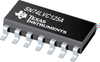

The SN74LVC125A is a quadruple bus buffer gate featuring 3-state outputs, designed for operation within a voltage range of 1.65V to 3.6V. It includes independent line drivers, each with a separate output-enable (OE) input, allowing for flexible control of the output states. The device is capable of accepting input voltages up to 5.5V, making it suitable for use in mixed 3.3V and 5V systems, which can be beneficial for signal translation applications. This component is specified for operation across a temperature range of -40°C to 125°C, ensuring reliability in various environmental conditions. The maximum propagation delay (t_pd) is 4.8ns at 3.3V, with low output ground bounce (V_OLP) and undershoot (V_OHV) characteristics, enhancing signal integrity. The SN74LVC125A is suitable for a wide range of applications, including telecom systems, optical networking, and various communication devices.
Quadruple Bus Buffer Gate With 3-State Outputs 14-SOIC -40 to 125
| Texas Instruments | |
|---|---|
| Product Category | IC Interfaces |
| Product Number | SN74LVC125ADG4 |
| Product Name | SN74LVC125A Quadruple Bus Buffer Gate With 3-State Outputs |
| Technology | LVC |
| Device Type | Buffer |
| Features | RoHS |


