Texas Instruments SN74GTL16616 17-Bit LVTTL-To-GTL/GTL+ Universal Bus Transceivers With Buffered Clock Outputs SN74GTL16616DGGR

Description
17-Bit LVTTL-To-GTL/GTL+ Universal Bus Transceivers With Buffered Clock Outputs 56-TSSOP -40 to 85
Request a Quote
Description
17-Bit LVTTL-To-GTL/GTL+ Universal Bus Transceivers With Buffered Clock Outputs 56-TSSOP -40 to 85
Request a Quote
Datasheet
Datasheet Summary
Powered by GS/AI

The SN74GTL16616 is a 17-bit LVTTL-to-GTL/GTL+ universal bus transceiver with buffered clock outputs, designed for signal-level translation between LVTTL and GTL/GTL+ logic levels. It is packaged in a 56-pin TSSOP (DGG) format and operates over a temperature range of -40°C to 85°C. The device supports mixed-mode operation with a 5-V-tolerant A-port and GTL/GTL+ on the B-port, using a reference voltage (VREF) settable to 1.2 V or 1.5 V for GTL or GTL+ modes. It features bus-hold circuitry on A-port inputs, OEC™ circuitry for improved signal integrity, and I_off circuitry to support partial-power-down operation. The transceiver includes dual-clock and dual-output-enable controls for bidirectional data flow, with a buffered GTL/GTL+ clock output (CLKOUT). Latch-up performance exceeds 100 mA per JESD78, Class II, and ESD protection exceeds 2000 V human-body model per JESD22-A114-A.

Suppliers

Company
Product
Description
Supplier Links
SN74GTL16616 17-Bit LVTTL-To-GTL/GTL+ Universal Bus Transceivers With Buffered Clock Outputs - SN74GTL16616DGGR - Texas Instruments
Dallas, TX, United States
SN74GTL16616 17-Bit LVTTL-To-GTL/GTL+ Universal Bus Transceivers With Buffered Clock Outputs
SN74GTL16616DGGR
SN74GTL16616 17-Bit LVTTL-To-GTL/GTL+ Universal Bus Transceivers With Buffered Clock Outputs SN74GTL16616DGGR
17-Bit LVTTL-To-GTL/GTL+ Universal Bus Transceivers With Buffered Clock Outputs 56-TSSOP -40 to 85

17-Bit LVTTL-To-GTL/GTL+ Universal Bus Transceivers With Buffered Clock Outputs 56-TSSOP -40 to 85

Buy Now Datasheet

Technical Specifications

  Texas Instruments
Product Category Logic Level Translators
Product Number SN74GTL16616DGGR
Product Name SN74GTL16616 17-Bit LVTTL-To-GTL/GTL+ Universal Bus Transceivers With Buffered Clock Outputs
Logic Family TTL; GTL
Package Type SSOP,TSSOP
Input Voltage 3.15 to 5.25 volts
Unlock Full Specs
to access all available technical data

Similar Products

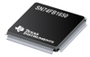
SN74FB1650 18-Bit TTL/BTL Universal Storage Transceiver - SN74FB1650PCA - Texas Instruments
Specs
Logic Family TTL
Package Type HLQFP
Input Voltage 4.5 to 5.5 volts
View Details
Translators, Level Shifters - 100324J-QMLV - Quarktwin Technology Ltd.
Specs
Package Type DIP; 24-CDIP (0.400\", 10.16mm)
Output Type Differential
Features RoHS
View Details
2 suppliers
SN74FB1653 17-Bit LVTTL/BTL Universal Storage Transceivers With Buffered Clock Lines - SN74FB1653PCA - Texas Instruments
Specs
Logic Family TTL
Package Type HLQFP
Input Voltage 4.5 to 5.5 volts
View Details