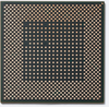
This is a semiconductor chip with a size that is more than 80% of the finished part.
It is called FCCSP (Flip Chip CSP) as flip chip bumps are used. It is mainly used for the AP (Application Processor) chips of mobile IT devices.
General Features
High performance : High performance is realized through the minimization of the Chip ↔ PCB distance that results in less signal loss
High I/O : I/O is formed in large quantities due to microbump pitch
Application
Mobile Application Processor, Baseband and Others
Why Samsung
Features of Products (Technology)
Different from wire bonding, input and output are formed on the semiconductor (chip) through an area array, and then the chip is flipped and connected to the PCB
Compared with WBCSP that uses gold wire, the path distance of electric signals is short, and input and output can be formed in large quantities, allowing the product to handle high-density semiconductors.
SPVF
With the SPVF (Samsung Photo Via Film) material, the quality of the product is guaranteed.
Laser via-less process
High productivity of via process (similar to Litho process)
Fine Line/Space
Competitive cost of process and material
Properties of SPVF
Item
Unit
Method/Condition
Samsung Photo Via Film
Quality
SiO2 Content
wt%
TGA
40
CTE
α1, ppm/℃
TMA
42
α2, ppm/℃
TMA
118
Tg
℃
TMA
172
Young’s Modulus
㎬
UTM
4.7
Tensile Strength
㎫
UTM
81
Elongation
%
UTM
3.4
Water absorption
wt%
100℃, 1h
0.9
Process-ability
Via Formation
Photo-Via
Melt Viscosity
Pas
Rheometer, (80℃)
141
Max. Resolution
㎛
20 ㎛T, 250mJ
50
Via Taper
%
@Max. Resolution
Min 70
Ra
㎛
Desmear (S/P/A=5/7/5)
0.24
Cu Peel
㎏f/㎝
E’less Cu : 1 ㎛ Electro Cu : 30 ㎛
Min 0.45
Cz Peel
㎏f/㎝
Cu foil : 30 ㎛
0.70
BSP
For the first time in the world, BSP (Blue Stencil Printing) method is applied to mass production
Available for fine bump pitch
Good for small bump risk
High productivity of bump processing
Competitive price by high productivity & high yield
EPS
EPS (Embedded Passive Substrate) is a substrate that has an internally embedded semiconductor passive component.
The decoupling capacitor is normally used to stabilize the power supply voltage level. When embedded inside a substrate, power ground/network inductance can be reduced.
This is a semiconductor chip with a size that is more than 80% of the finished part.
It is called FCCSP (Flip Chip CSP) as flip chip bumps are used. It is mainly used for the AP (Application Processor) chips of mobile IT devices.
General Features
- High performance : High performance is realized through the minimization of the Chip ↔ PCB distance that results in less signal loss
- High I/O : I/O is formed in large quantities due to microbump pitch
Application
- Mobile Application Processor, Baseband and Others
Why Samsung
Features of Products (Technology)
Different from wire bonding, input and output are formed on the semiconductor (chip) through an area array, and then the chip is flipped and connected to the PCB
Compared with WBCSP that uses gold wire, the path distance of electric signals is short, and input and output can be formed in large quantities, allowing the product to handle high-density semiconductors.
SPVF
With the SPVF (Samsung Photo Via Film) material, the quality of the product is guaranteed.
- Laser via-less process
- High productivity of via process (similar to Litho process)
- Fine Line/Space
- Competitive cost of process and material
Properties of SPVF
| Item | Unit | Method/Condition | Samsung Photo Via Film |
|---|
| Quality | SiO2 Content | wt% | TGA | 40 |
|---|
| CTE | α1, ppm/℃ | TMA | 42 |
| α2, ppm/℃ | TMA | 118 |
| Tg | ℃ | TMA | 172 |
| Young’s Modulus | ㎬ | UTM | 4.7 |
| Tensile Strength | ㎫ | UTM | 81 |
| Elongation | % | UTM | 3.4 |
| Water absorption | wt% | 100℃, 1h | 0.9 |
| Process-ability | Via Formation | Photo-Via |
|---|
| Melt Viscosity | Pas | Rheometer, (80℃) | 141 |
| Max. Resolution | ㎛ | 20 ㎛T, 250mJ | 50 |
| Via Taper | % | @Max. Resolution | Min 70 |
| Ra | ㎛ | Desmear
(S/P/A=5/7/5) | 0.24 |
| Cu Peel | ㎏f/㎝ | E’less Cu : 1 ㎛
Electro Cu : 30 ㎛ | Min 0.45 |
| Cz Peel | ㎏f/㎝ | Cu foil : 30 ㎛ | 0.70 |
BSP
For the first time in the world, BSP (Blue Stencil Printing) method is applied to mass production
- Available for fine bump pitch
- Good for small bump risk
- High productivity of bump processing
- Competitive price by high productivity & high yield
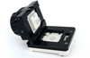
EPS
EPS (Embedded Passive Substrate) is a substrate that has an internally embedded semiconductor passive component.
The decoupling capacitor is normally used to stabilize the power supply voltage level. When embedded inside a substrate, power ground/network inductance can be reduced.