
The TW9990 is a low power NTSC/PAL/SECAM video decoder chip that is designed for automotive applications. It supports both single-ended and differential composite video as well as S-Video. Typical power consumption is 110mW for composite input applications, and the available power-down mode further reduces power consumption. It uses 1.8V for both analog and digital supply voltage and 3.3V for I/O power. A single 27MHz crystal is all that is needed to decode all analog video standards.
The video decoder converts base-band analog CVBS or S-Video signals into digital 8-bit 4:2:2 YCbCr video output format. It consists of an analog fron-end with input source selection, variable gain amplifier, analog-to-digital converters, a Y/C separation circuit, a multistandard color decoder (PAL BGHI, PAL M, PAL N, combination PAL N, NTSC M, NTSC 4.43 and SECAM), and synchronization circuitry. The Y/C separation is done with a high quality adaptive 4H comb filter for reduced cross color and cross luminance. The advanced synchronization processing circuitry can produce stable pictures for nonstandard and weak signals. The output of the decoder is line-locked and formatted to the ITU-R 656 output stardard with embedded sync.
The TW9990 also includs circuits to detect and process Vertical Blanking Interval (VBI) signals. It slices and processes VBI data for output through the video bus. Some information can also be retreived through the host interface.
A 2-wire serial host interface is used to simplify system integration and all functions can be controlled through this interface.
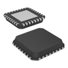
Video Decoder IC Video 32-QFN (5x5)
| Renesas Electronics Corporation | DigiKey | |
|---|---|---|
| Product Category | Logic Decoders and Demultiplexers | Logic Decoders and Demultiplexers |
| Product Number | TW9990AT-NA1-GR | TW9990AT-NA1-GR-ND |
| Product Name | Low Power NTSC/PAL/SECAM Video Decoder with Differential CVBS Inputs | Encoders, Decoders, Converters |
| Function | Decoder | Decoder |