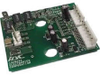

The SPDT Switch Evaluation Kit board was designed to ease customer evaluation of the PE4257 SPDT switch. The RF common port is connected through a 50 Ω transmission line to J2. Port 1 and Port 2 are connected through 50 Ω transmission lines to J1 and J3. A through transmission line connects SMA connectors J4 and J5. This transmission line can be used to estimate the loss of the PCB over the environmental conditions being evaluated. The board is constructed of a four metal layer FR4 material with a total thickness of 0.031”. The transmission lines were designed using a coplanar waveguide with ground plane (28 mil core, 47.6 mil width, 30mil gap). Note the number of vias surrounding the device in the layout. These vias are critical for obtaining the specified isolation performance for the device shown in this datasheet. J6 provides a means for controlling DC and digital inputs to the device. The provided jumpers short the package pin to ground for logic low. When the jumper is removed, the pin is pulled up to VDD for logic high. When the jumper is in place, 3 µA of current will flow through the 1 MΩ pull up resistor. This extra current should not be attributed to the requirements of the device.
Manufacturer: Peregrine Semiconductor
Win Source Part Number: 1087307-4257-00
Type: Switch, SPDT
For Use With/Related Products: PE4257
Frequency: 0Hz to 3GHz
Supplied Contents: Board
Categories: RF/IF and RFID
Status: Active
Popularity: Medium
Fake Threat In the Open Market: 56 pct.
Supply and Demand Status: Sufficient
KIT EVAL FOR 4257 RF SWITCH
| Richardson RFPD | Win Source Electronics | Acme Chip Technology Co., Limited | |
|---|---|---|---|
| Product Category | Electronic Development Boards | Electronic Development Boards | Electronic Development Boards |
| Product Number | 4257-00 | 1087307-4257-00 | 4257-00 |
| Product Name | Switch Evaluation Board | RF Evaluation and Development Kits, Boards - 4257-00 | Development Boards, Kits, Programmers - Evaluation Boards - RF Evaluation and Development Kits, Boards |
| Category | Developement Board | Developement Board | Developement Board |